 ALLPCB


In today's fast-paced world of electronics, high-speed PCB designs are at the heart of cutting-edge technology. From telecommunications to aerospace, engineers rely on these boards to handle signals racing at gigahertz (GHz) speeds. But as signal frequencies climb, so do the challenges. One of the biggest hurdles? Maintaining signal integrity through precise impedance control. Without it, reflections, crosstalk, and electromagnetic interference (EMI) can degrade performance or even cause system failure.
At its core, impedance control is about ensuring that PCB traces act as reliable transmission lines for high-speed signals. It's a critical factor that separates a functional design from one plagued by errors. In this blog, we'll break down what impedance control is, why it matters, and how engineers can achieve precision in their high-speed PCB designs. Whether you're routing a differential pair for USB or designing a multi-layer board for 5G, these insights will help you get it right.
What Is Impedance Control in PCB Design?
Impedance control refers to the process of managing the electrical impedance of PCB traces to match the requirements of the components and signals they connect. Impedance, measured in ohms (Ω), is the opposition a circuit presents to alternating current (AC), combining resistance, inductance, and capacitance. In high-speed designs, PCB traces aren't just simple conductors—they behave like transmission lines where impedance must remain consistent to prevent signal distortion.
For example, a USB 2.0 differential pair typically requires a 90Ω impedance, while a single-ended trace for DDR memory might need 50Ω. If the impedance deviates—say, due to inconsistent trace width or poor layer stack-up—part of the signal reflects back, causing issues like overshoot or data errors. Controlled impedance ensures that signals travel from source to load with minimal loss or interference,
Why Impedance Control Matters in High-Speed Designs
As signal speeds increase, the electrical length of a trace becomes a significant factor. A general rule of thumb is that impedance control becomes critical when a trace's length exceeds one-sixth of the signal's rise time (converted to distance). For a 1 ns rise time signal traveling at 6 inches per nanosecond, that's about 1 inch. Beyond this, reflections and timing issues creep in.
High-speed applications—like 10 Gbps Ethernet or HDMI—demand precision because even small impedance mismatches can lead to catastrophic signal degradation. For instance, a 10% mismatch in a 50Ω trace (5Ω off) can reflect enough energy to corrupt data. Additionally, crosstalk between adjacent traces and EMI from poor grounding can amplify these problems. Controlled impedance mitigates these risks by ensuring uniformity along the trace, preserving signal integrity and system reliability.
Beyond functionality, impedance control impacts manufacturing consistency. Without clear specifications, boards from different runs might vary, complicating debugging and quality control. For engineers, mastering impedance control is a non-negotiable skill in modern PCB design.
Key Factors Affecting Impedance in PCB Traces
Achieving precise impedance control starts with understanding what influences it. Here are the primary factors engineers must consider:
1. Trace Geometry
- Width and Thickness: Wider and thicker traces lower impedance. For a 50Ω microstrip on FR-4, a typical width might be 7 mils with a 1 oz copper thickness (1.4 mils).
- Length: While length doesn't directly affect characteristic impedance, it impacts signal timing and loss over distance.
Suggested Reading: Unlocking Signal Integrity: A Deep Dive into FR-4 PCB Trace Impedance Control
2. Dielectric Material
- The dielectric constant (Dk) of the PCB substrate—like FR-4 (Dk ≈ 4.3) or Megtron 6 (Dk ≈ 3.4)—inversely affects impedance. Lower Dk materials increase impedance and reduce signal loss, ideal for GHz-range designs.
3. Layer Stack-Up
- The distance between a signal trace and its reference plane (ground or power) is crucial. A thinner dielectric (e.g., 4 mils) increases capacitance, lowering impedance, while a thicker one (e.g., 10 mils) raises it.
Suggested Reading: Cost-Effective Stackup Strategies for Impedance Controlled PCBs
4. Trace Spacing
- In differential pairs, spacing between traces affects differential impedance. For a 100Ω pair, spacing might be 8 mils, depending on stack-up and material.
5. Manufacturing Tolerances
- Etching precision, copper thickness variations, and dielectric consistency can shift impedance by ±10% or more if not tightly controlled.
Steps to Achieve Precision Impedance Control
Now that we've covered the basics, let's dive into actionable steps to design a high-speed PCB with controlled impedance.
Step 1: Define Impedance Requirements
Start by identifying the impedance targets for your design. Common standards include:
- Single-Ended: 50Ω (e.g., RF signals, DDR).
- Differential: 90Ω (USB), 100Ω (LVDS), or 120Ω (Ethernet).
Check component datasheets and interface specifications to confirm these values. For example, a 10 Gbps SerDes might specify 100Ω ± 10%.
Step 2: Design the Layer Stack-Up
Collaborate with your PCB manufacturer to create a stack-up that supports your impedance goals. A 4-layer PCB might use:
- Top layer: Signal traces.
- Layer 2: Ground plane.
- Layer 3: Power plane.
- Bottom layer: Signal traces.
For higher speeds (e.g., 10 Gbps+), an 8-layer stack-up with interleaved ground planes between signal layers reduces crosstalk and EMI. Specify dielectric thickness and material—Megtron 6, for instance, excels at minimizing signal loss above 5 GHz.
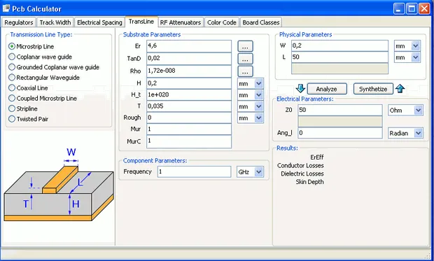
Step 3: Calculate Trace Geometry
Use an impedance calculator or field solver (available in tools like Altium Designer or Sierra Circuits' Impedance Calculator) to determine trace width and spacing. For a 50Ω microstrip on a 10-mil FR-4 dielectric, you might need a 18-mil-wide trace. Differential pairs require additional spacing rules—e.g., 8 mils apart for 100Ω on the same stack-up.
Step 4: Route with Precision
- Maintain Consistency: Avoid abrupt changes in trace width or gaps in reference planes, as these cause impedance discontinuities.
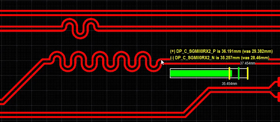
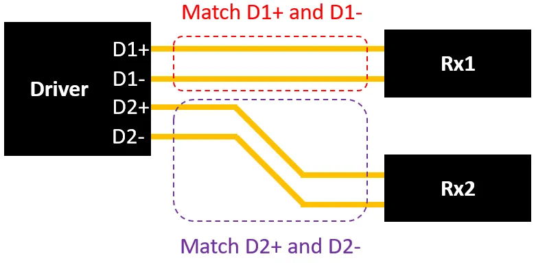
- Length Matching: For differential pairs or parallel buses, match trace lengths within 20% of the signal rise time (e.g., 0.2 inches for a 1 ns rise time) to prevent skew.
- Avoid Vias Where Possible: Vias introduce inductance and capacitance, altering impedance. If unavoidable, use back-drilling to remove stubs in high-speed designs.
Step 5: Specify Fabrication Notes
Clearly annotate your PCB design files with impedance requirements. For example:
- "Layer 1: 7-mil traces, 50Ω ± 10% single-ended."
- "Layers 1-2 dielectric: 10 mils, FR-4, Dk = 4.3."
Include a stack-up table and request test coupons—small trace segments on the panel—for impedance verification.
Step 6: Verify with Testing
Manufacturers use Time Domain Reflectometry (TDR) to measure impedance on test coupons or actual traces. A TDR sends a pulse down the trace and analyzes reflections to confirm the impedance matches your spec (e.g., 50Ω ± 5Ω). Review these reports to ensure consistency across production runs.
Common Challenges and Solutions
Even with careful planning, impedance control can trip up engineers. Here are some pitfalls and how to tackle them:
Challenge 1: Material Variability
- Problem: Dielectric constants vary between batches (e.g., FR-4's Dk can range from 4.2 to 4.6).
- Solution: Specify a controlled dielectric approach, locking in Dk and thickness with your manufacturer. Opt for low-Dk materials like Rogers 4350B for critical designs.
Challenge 2: Manufacturing Tolerances
- Problem: Etching undercut or copper thickness variation shifts impedance by 3-5Ω.
- Solution: Request tight tolerances (e.g., ±5%) and review the manufacturer's process capabilities. Use wider traces where possible to reduce sensitivity to etching errors.
Challenge 3: EMI and Crosstalk
- Problem: Adjacent high-speed traces interfere, especially in dense layouts.
- Solution: Increase spacing (e.g., 3x the trace width) and add ground planes or guard traces. Simulate with tools like HyperLynx to predict and mitigate EMI.
Best Practices for High-Speed PCB Design
To round out your approach, adopt these proven strategies:
- Simulate Early: Use signal integrity tools to model impedance and reflections before fabrication.
- Collaborate with Fabricators: Share your stack-up and impedance goals early to align on materials and tolerances.
- Test Thoroughly: Beyond TDR, perform functional tests at target frequencies (e.g., 2.4 GHz for Wi-Fi) to catch real-world issues.
- Document Everything: Detailed notes and design rules ensure repeatability across revisions and manufacturers.
Suggested Reading: PCB Stackup Design: The Key to Impedance Control
How ALLPCB Supports Impedance Control
For engineers tackling high-speed designs, partnering with a capable manufacturer is key. ALLPCB offers advanced fabrication capabilities tailored to impedance-controlled PCBs. Our quick-turn prototyping delivers boards in as little as 24 hours, letting you test and refine designs fast. Whether you're prototyping a 5G module or scaling up production, we've got the tools and know-how to support your success.
Conclusion
Impedance control is the backbone of high-speed PCB design, ensuring signals stay clean and systems perform reliably. By defining clear requirements, designing a robust stack-up, calculating precise trace geometries, and working closely with your manufacturer, you can achieve the precision today's applications demand. From 50Ω RF traces to 100Ω LVDS pairs, every detail counts—and getting it right pays off in performance and peace of mind.
As signal speeds push past 10 Gbps and beyond, mastering impedance control isn't just a skill—it's a necessity. Armed with these steps and best practices, you're ready to design PCBs that meet the toughest challenges head-on. Ready to start? Dive into your next high-speed project with confidence.


