ALLPCB


If you're an electrical engineer working in PCB assembly, stencil printing defects can be a major roadblock, causing issues like solder bridging, insufficient solder, or solder paste smearing. These problems can lead to costly rework or even product failures. So, how do you troubleshoot and fix these issues? In this practical guide, we’ll walk you through the most common stencil printing defects, their causes, and actionable solutions to ensure a smooth PCB assembly process. Whether you're dealing with stencil alignment issues or uneven solder deposits, we've got you covered with detailed steps and tips tailored for engineers like you.
Introduction to Stencil Printing in PCB Assembly
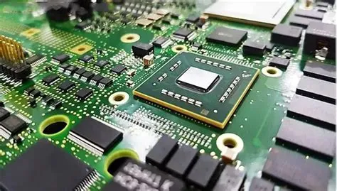
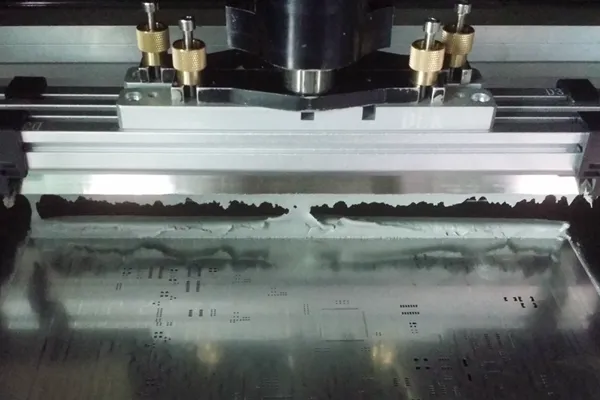
Stencil printing is a critical step in surface mount technology (SMT) during PCB assembly. It involves depositing solder paste onto the PCB through a stencil—a thin metal sheet with precisely cut apertures corresponding to the component pads. This process sets the foundation for proper soldering and component placement. However, even small errors in stencil printing can lead to defects that affect the entire assembly process. Issues like solder bridging, insufficient solder, or stencil alignment problems can result in poor connections, shorts, or component failures.
In this blog, we’ll dive deep into troubleshooting common stencil printing defects. Our goal is to equip you with practical knowledge and solutions to identify, fix, and prevent these issues in your PCB assembly workflow. Let’s start by understanding the most frequent problems engineers face during stencil printing.
Common Stencil Printing Defects in PCB Assembly
Before we jump into troubleshooting, let’s break down the most common stencil printing defects you’re likely to encounter. Each defect has specific causes and impacts on the final PCB quality. Understanding these will help you diagnose issues faster and apply the right fixes.
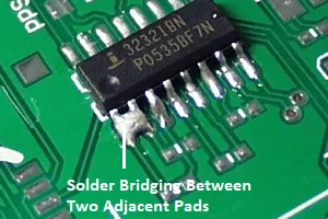
1. Solder Bridging
Solder mask bridge occurs when excess solder paste connects two adjacent pads, creating an unintended electrical short after reflow. This defect is often visible as a "bridge" of solder between pads and can lead to circuit malfunctions.
Causes:
- Overly large stencil apertures depositing too much solder paste (e.g., apertures 10-20% larger than pad size).
- Stencil misalignment causing paste to spread beyond pad boundaries.
- Excessive squeegee pressure during printing, forcing paste under the stencil.
Impact: Solder bridging can cause short circuits, leading to functional failures in devices. For high-density boards with fine-pitch components (e.g., 0.4mm pitch), this defect is especially problematic.
2. Insufficient Solder
Insufficient solder happens when too little solder paste is deposited on the pads, resulting in weak or incomplete solder joints after reflow. This defect often leads to poor mechanical and electrical connections.
Causes:
- Undersized or clogged stencil apertures, restricting paste flow (e.g., apertures blocked by dried paste or debris).
- Low squeegee pressure, failing to push enough paste through the stencil.
- Worn-out or damaged stencils with uneven aperture walls.
Impact: Weak solder joints can fail under thermal or mechanical stress, causing intermittent connections or complete component detachment.
3. Solder Paste Smearing
Solder paste smearing refers to the unintended spread of paste outside the pad areas, often creating messy deposits that can lead to bridging or uneven joints.
Causes:
- Poor stencil-to-PCB contact, allowing paste to seep under the stencil.
- Excessive squeegee speed (e.g., above 50mm/s for some setups), causing paste to drag across the stencil.
- Inadequate cleaning of the stencil, leaving residue that mixes with fresh paste.
Impact: Smearing increases the risk of shorts and inconsistent solder volume, affecting the reliability of the assembly.
4. Stencil Alignment Issues
Stencil alignment issues occur when the stencil apertures do not align perfectly with the PCB pads, leading to misplaced solder paste deposits.
Causes:
- Inaccurate fiducial mark detection during setup, causing misalignment by as little as 0.1mm.
- Warped or stretched stencils due to prolonged use or improper handling.
- PCB dimensional variations or poor clamping in the printer.
Impact: Misaligned paste can result in insufficient solder on pads or paste on unintended areas, leading to soldering defects and rework.
Troubleshooting Stencil Printing Defects: Step-by-Step Solutions
Now that we’ve identified the common stencil printing defects, let’s explore practical troubleshooting steps for each issue. These solutions are designed to help electrical engineers like you resolve problems quickly and prevent them from recurring in future PCB assembly runs.
Troubleshooting Solder Bridging
Step 1: Inspect Stencil Design
Check if the stencil apertures are oversized. For fine-pitch components, ensure the aperture size is reduced by 10-15% compared to the pad size to control paste volume. Use a stencil design tool or consult your stencil manufacturer for precise aperture dimensions.
Step 2: Adjust Squeegee Pressure
Excessive squeegee pressure can force paste under the stencil, causing bridging. Reduce pressure to a range of 0.2-0.3 kg/cm of squeegee blade length, depending on your printer model, and test the results. Monitor for consistent paste deposits without overflow.
Step 3: Verify Stencil Alignment
Use the printer’s vision system to confirm stencil-to-PCB alignment. Misalignment by even 0.05mm can lead to bridging on fine-pitch pads. Recalibrate fiducial marks if necessary.
Prevention Tip: Regularly inspect stencils for wear and replace them after 50,000-100,000 prints, depending on usage and material (e.g., stainless steel stencils last longer than nickel).
Troubleshooting Insufficient Solder
Step 1: Check for Clogged Apertures
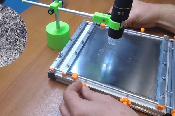
Inspect the stencil for blockages using a magnifying glass or automated optical inspection (AOI). Clean clogged apertures with isopropyl alcohol and a soft brush, or use an ultrasonic cleaner for stubborn residue. For fine-pitch apertures (e.g., 0.3mm), consider a stencil with laser-cut openings for smoother walls.
Step 2: Optimize Squeegee Pressure and Angle
Increase squeegee pressure slightly (e.g., to 0.3-0.4 kg/cm) to ensure adequate paste transfer. Also, adjust the squeegee angle to 45-60 degrees for better paste rolling and deposition.
Step 3: Evaluate Solder Paste Condition
Old or dried-out solder paste may not flow properly. Check the paste’s expiration date and storage conditions (typically 4-10°C). Use fresh paste if viscosity exceeds manufacturer specs (e.g., 600-1200 kcps for Type 3 paste).
Prevention Tip: Implement a regular stencil cleaning schedule (e.g., after every 5-10 prints) to avoid paste buildup in apertures.
Troubleshooting Solder Paste Smearing
Step 1: Ensure Proper Stencil-to-PCB Contact
Verify that the PCB is securely clamped and flat against the solder paste stencil. Any gap (even 0.1mm) can cause smearing. Adjust the printer’s snap-off distance to 0mm or use a slight negative snap-off for better contact.
Step 2: Reduce Squeegee Speed
Lower the squeegee speed to 20-40mm/s to minimize paste dragging. Test different speeds to find the optimal setting for your paste type and stencil thickness (e.g., 100-150μm).
Step 3: Clean Stencil Regularly
Smearing often results from residual paste on the stencil underside. Wipe the stencil with a lint-free cloth and solvent after every 5-10 prints, or use an automated under-stencil cleaning system for high-volume production.
Prevention Tip: Store stencils in a clean, dust-free environment to avoid contamination that could contribute to smearing.
Troubleshooting Stencil Alignment Issues
Step 1: Recalibrate Printer Vision System
Use the printer’s software to recalibrate fiducial mark detection. Ensure the camera system accurately identifies marks on both the PCB and stencil. A misalignment of 0.025mm can cause noticeable paste offset on fine-pitch pads.
Step 2: Inspect Stencil for Warping
Check if the stencil is warped or stretched by laying it flat on a surface or using a tension meter (target tension: 35-40 N/cm for stainless steel stencils). Replace warped stencils immediately.
Step 3: Verify PCB Dimensions
Measure the PCB for dimensional accuracy using a caliper or coordinate measuring machine (CMM). Variations beyond ±0.1mm from the design file can cause alignment issues. Work with your PCB supplier to ensure tight tolerances.
Prevention Tip: Use stencils with etched fiducial marks for better alignment accuracy, and store them properly to avoid physical distortion.
Best Practices for Preventing Stencil Printing Defects
While troubleshooting is essential, preventing stencil printing defects in the first place saves time and reduces rework costs. Here are some best practices for maintaining a defect-free PCB assembly process:
- Regular Maintenance: Schedule routine maintenance for your stencil printer, including squeegee blade replacement (every 3-6 months) and vision system calibration (monthly).
- Stencil Quality: Invest in high-quality laser-cut stencils with smooth aperture walls and precise dimensions. For fine-pitch components, opt for stencils with a thickness of 80-100μm.
- Solder Paste Handling: Store solder paste at the recommended temperature (4-10°C) and allow it to reach room temperature (20-25°C) for 4-6 hours before use to avoid condensation and viscosity issues.
- Process Monitoring: Use automated optical inspection (AOI) or solder paste inspection (SPI) systems to detect defects immediately after printing. Modern SPI machines can measure paste volume with an accuracy of ±5%.
- Training: Ensure operators are trained on proper printer setup, stencil handling, and cleaning procedures to minimize human error.
Real-World Example: Solving a Solder Bridging Issue
During a recent PCB assembly project for a high-density IoT device, our team encountered frequent solder bridging on 0.5mm pitch QFN components. After inspection, we found that the stencil apertures were 15% larger than optimal, depositing excess paste. We worked with the stencil manufacturer to redesign the apertures with a 10% reduction and adjusted the squeegee pressure from 0.4 kg/cm to 0.25 kg/cm. Additionally, we implemented an SPI system to verify paste volume after printing. These changes reduced bridging defects by 90% in subsequent runs, saving hours of rework.
This example shows how a combination of design adjustments and process optimization can address stencil printing defects effectively. Tailor these strategies to your specific setup for similar results.
Conclusion: Mastering PCB Assembly Troubleshooting
Stencil printing defects like solder bridging, insufficient solder, solder paste smearing, and stencil alignment issues can disrupt your PCB assembly process, but they’re not insurmountable. By understanding the root causes and applying the troubleshooting steps outlined in this guide, you can minimize defects and improve the reliability of your assemblies. Remember to focus on prevention through regular maintenance, high-quality materials, and process monitoring to avoid issues before they start.
As an electrical engineer, your expertise in diagnosing and fixing these problems is crucial for delivering high-quality electronics. Have you encountered any unique stencil printing challenges in your projects? Share your experiences or questions in the comments below—we’d love to help brainstorm solutions. For now, apply these practical tips to your next PCB assembly run and watch your defect rates drop!