 ALLPCB


After the PCB manufacturing is completed, the boards are sent to another building within our factory campus. This building is just a three-minute walk from our PCB production workshop, yet it houses completely different equipment, and the workers there perform entirely different tasks.
In this building, PCBs and components are assembled together. Automated machines work alongside workers to complete the assembly process at the fastest speed.
Today, we will introduce the machines in this building and the daily tasks carried out here. We believe that after reading this article, you will have a better understanding of our factory.
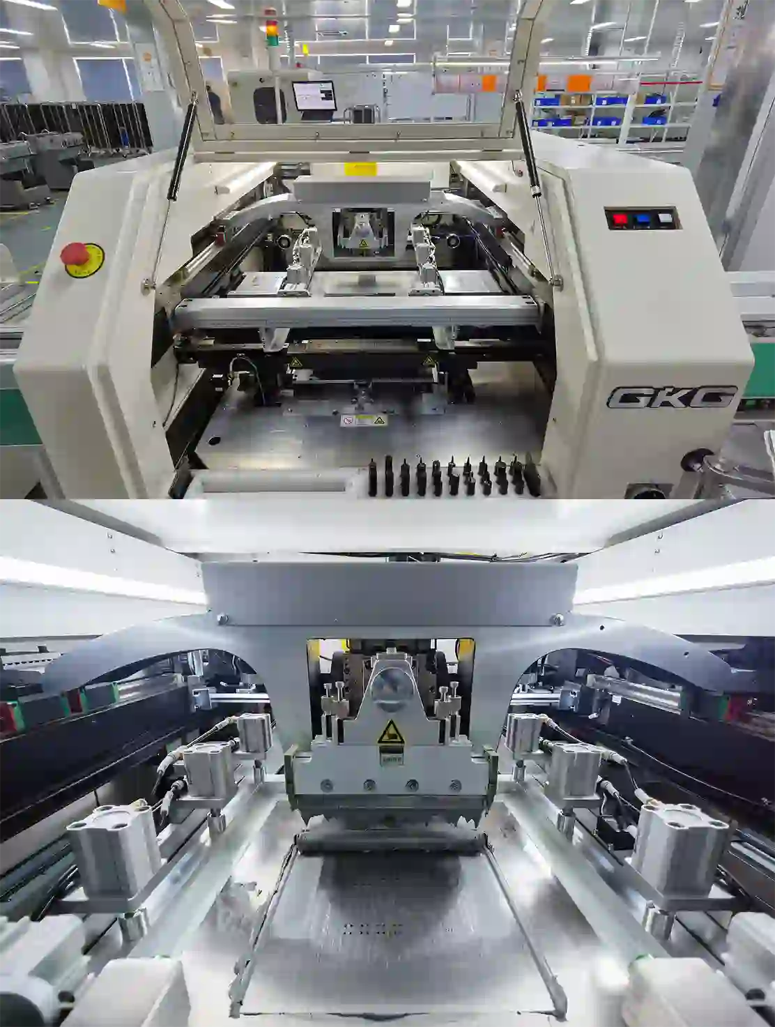
Solder Paste Stenciling
The first step of PCB assembly is applying a solder paste to the board. First, the workers connect the prepared automatic board loader to the front end of this machine. And then our workers place a pre-made stencil into the machine, which then automatically applies a layer of solder paste to each board.
After two quick passes of the scraper, a layer of solder paste has been applied to the board. Next, the board moves along the conveyor belt to the next process—the fully automated solder paste inspection (SPI) machine. In this machine, laser and 3D scanning technology are used to determine whether the solder paste on each pad meets process requirements.
After scanning for less than a minute, the machine will display either "Pass" or "Failed."
Pick and Place
After the SPI inspection, the board continues along the conveyor belt into the fully automated pick-and-place machine. Currently, at ALLPCB, we have seven Siemens high-speed and high-accuracy SMT production lines.
This equipment is the key to ensuring our fast delivery and is undoubtedly the king of this workshop! (By all means, even the cost of money)
After the workers have verified the components against the work order, they place the components onto the feeders. Once the feeders are loaded with the components required for the SMT process, the pick-and-place operation begins.
Reflow Soldering
Once the solder paste and surface mount components are properly positioned, they need to stay in place. To achieve this, the solder paste must solidify, bonding the components to the board. This process is known as "reflow" in PCB assembly.
After the pick-and-place step, the PCB is moved onto a conveyor belt, which carries it through a large reflow oven—similar to a commercial pizza oven:) This oven is equipped with a series of heaters that gradually raise the temperature of the board to about 250°C, which is hot enough to melt the solder in the paste.
As the solder melts, the PCB continues through the oven and passes through cooler heaters, which allow the molten solder to cool and solidify in a controlled manner. This forms a permanent solder joint that securely attaches the SMDs to the PCB.
Some PCBAs require special handling during reflow, particularly for two-sided PCB assembly. In these cases, each side is stenciled and reflowed separately. First, the side with fewer and smaller components is stenciled, placed, and reflowed, followed by the other side.
Inspection and Quality Control
After the surface mount components are soldered during the reflow process, the PCB assembly is not yet complete. The assembled board must undergo functionality testing. Movement during reflow can lead to poor connections or even a total lack of connection. Additionally, shorts are a common issue, as misaligned components can sometimes cause unintended connections between parts of the circuit that should remain separate.
Manual Checks: Despite the growing trend toward automated and smart manufacturing, manual checks remain a key part of the PCB assembly process. For smaller batches, visual inspection by a designer is an effective way to ensure the quality of a PCB after the reflow process. However, as the number of boards increases, this method becomes less practical and less accurate. Prolonged inspection of small components can lead to optical fatigue, diminishing the accuracy of the checks.
Automatic Optical Inspection (AOI): Automatic optical inspection is a more suitable method for inspecting larger batches of PCBs. The AOI machine uses high-powered cameras positioned at various angles to "view" the solder connections on the board. Different types of solder joints reflect light in distinct ways, allowing the AOI to identify lower-quality solder. This process is very fast, enabling it to handle a high volume of PCBs in a relatively short amount of time.
X-ray Inspection: Another inspection method involves the use of X-rays, which is less common but especially useful for complex or multi-layered PCBs. X-ray inspection allows a detailed view of the internal layers, making it possible to detect issues that might be hidden beneath the surface.
Through-Hole Component Insertion
After completing the SMT process, the next step we need to handle is THT.
A plated through-hole is a hole in the PCB that is coated with metal throughout its entire depth. These holes allow PCB components to transmit signals from one side of the board to the other. Unlike SMT, solder paste is ineffective here, as it would simply flow through the hole without adhering properly.
Manual Soldering: In manual through-hole insertion, workers place components into designated PTHs at individual stations. Each board moves sequentially through stations until all components are inserted. This process can be time-consuming, which is why many companies avoid designing with PTH components, though they remain common in PCB designs.
Wave Soldering: A more automated alternative, wave soldering involves placing the PTH components and then sending the board through a specialized oven on a conveyor belt. A wave of molten solder coats the bottom of the board, soldering all pins simultaneously. However, this method is impractical for double-sided PCBs, as it could damage delicate components.
Final Inspection and Functional Test
After soldering, a functional test ensures the PCB operates correctly. This test simulates real-world conditions by running power and signals through the board while monitoring electrical characteristics.
If voltage, current, or signal output deviates beyond acceptable limits, the PCB fails and is either recycled or scrapped per company standards.
The boards that pass inspection are sent to the final workshop — the packaging and shipping department. Workers carefully package the boards according to requirements. That evening, DHL or FedEx couriers will pick up your goods, and there's a good chance they'll be on a plane the very next day.
Conclusion
Ok, this is what we would like to introduce to you today!
I believe after reading this article, you must have gained a deeper understanding of PCBA and ALLPCB!
There are many more stories about our PCBA factory, and we will continue to share them with you in the future!


