 ALLPCB


In the fast-paced world of electronics manufacturing, printed circuit boards (PCBs) are the backbone of countless devices, from smartphones to medical equipment. Ensuring their quality is critical, as even a single defect can lead to costly failures or safety hazards. Automated Optical Inspection (AOI) has emerged as a cornerstone technology in PCB assembly, enabling manufacturers to detect defects with precision and efficiency. By leveraging advanced imaging and software, AOI ensures that every PCB meets stringent quality standards, reducing errors and boosting reliability. In this blog, we explore how AOI works, its benefits, and its indispensable role in modern PCB production.
What Is Automated Optical Inspection (AOI)?
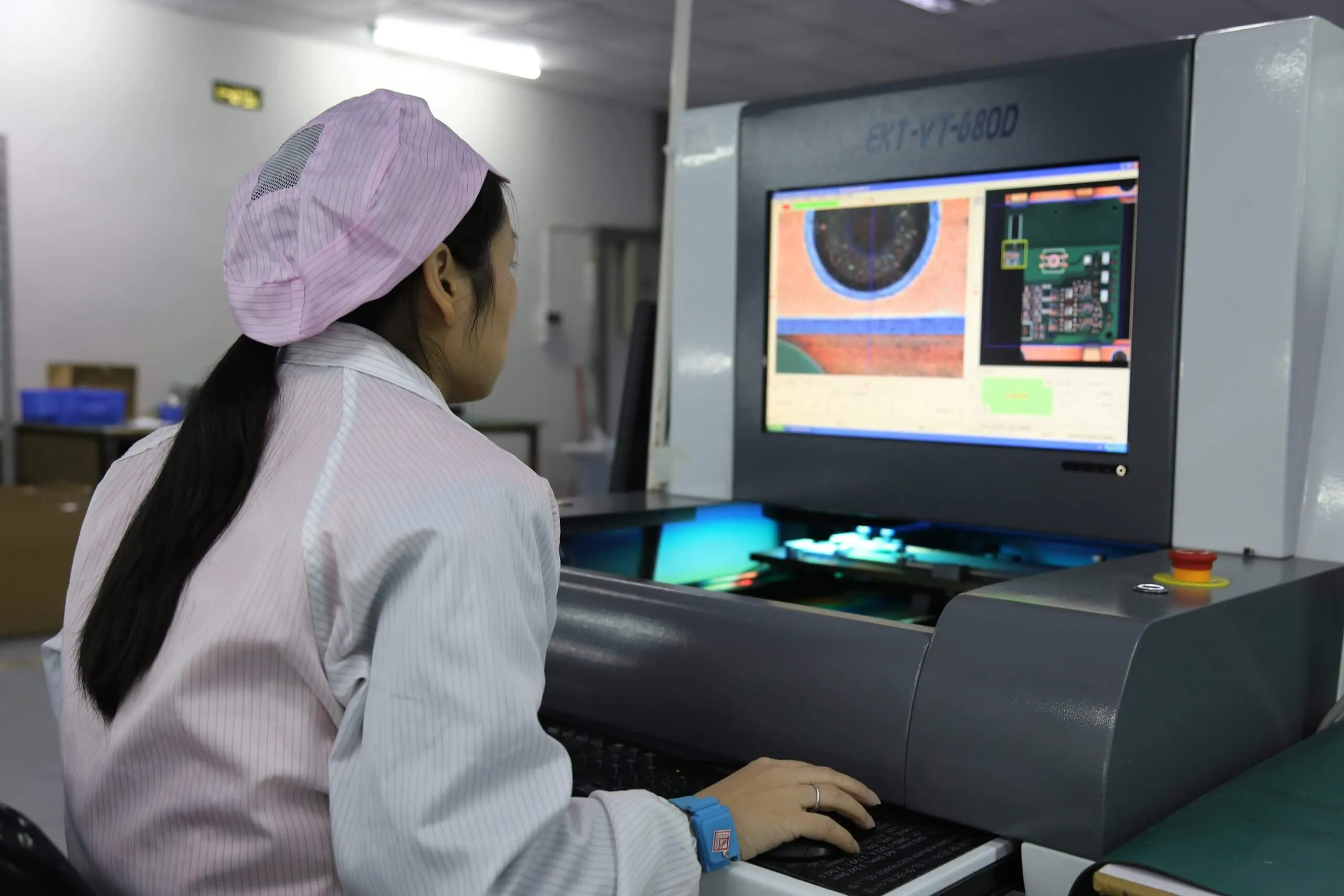
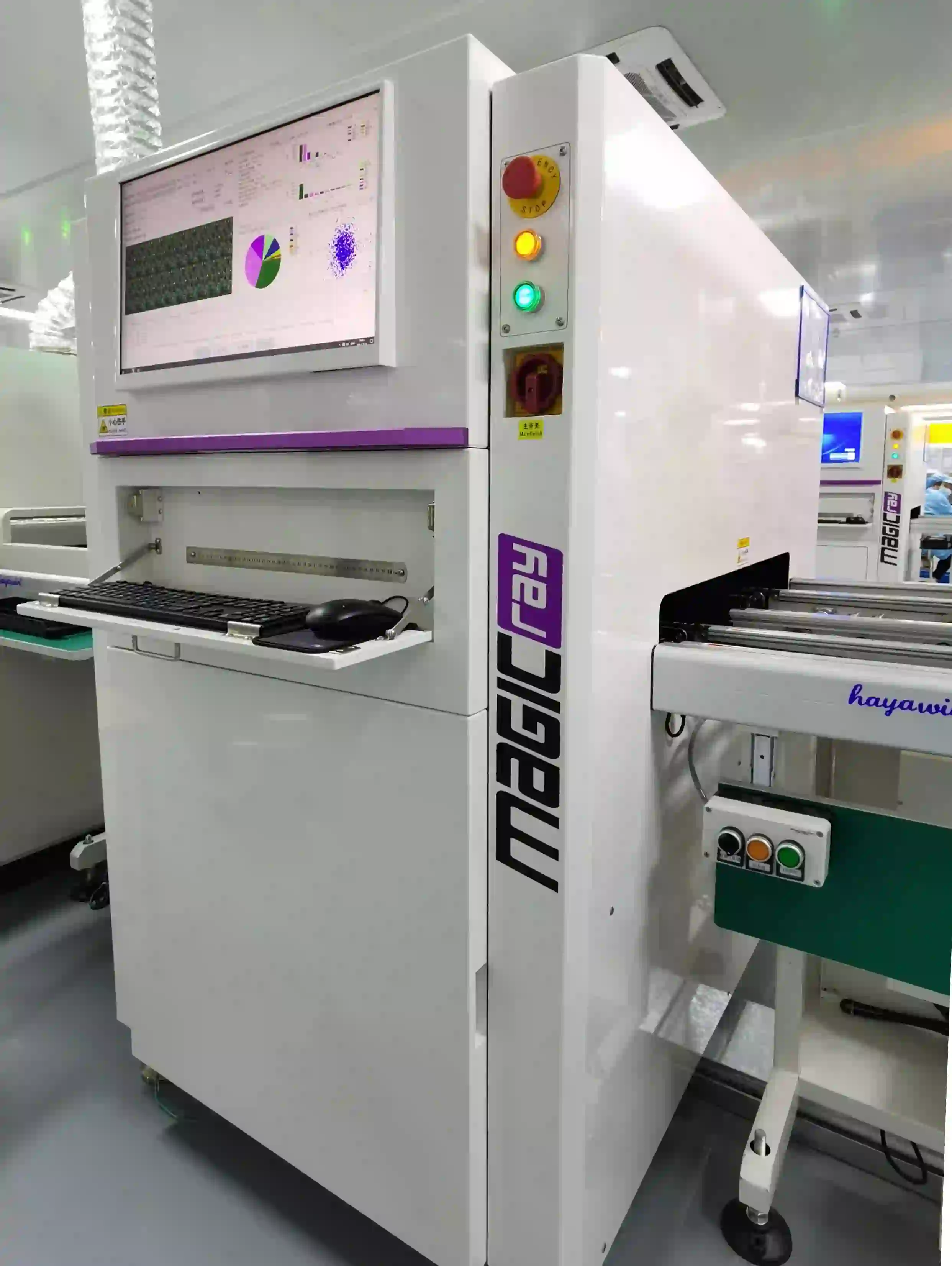
Automated Optical Inspection is a machine-based visual inspection technique used during PCB manufacturing and assembly to identify defects. Unlike manual inspection, which is time-consuming and prone to human error, AOI uses high-resolution cameras, sophisticated lighting, and image-processing software to scan PCBs for surface-level issues. These systems compare captured images against a 'golden standard'—a reference design or a pre-approved PCB—to flag discrepancies such as missing components, solder joint defects, or trace irregularities.
AOI is typically deployed at various stages of production, including after solder paste application, component placement, and reflow soldering. Its ability to inspect complex boards with thousands of solder joints and tiny components (e.g., 0201 or 01005 packages) makes it essential in today's high-density PCB designs. For example, a single 10 cm x 10 cm board may contain over 2,000 solder joints, making manual inspection impractical.
How AOI Works in PCB Assembly
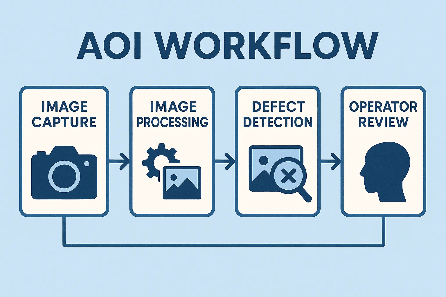
AOI systems operate through a combination of hardware and software designed for precision. Here's a breakdown of the process:
1. Image Acquisition
Multiple high-resolution cameras (often 5–15 megapixels) capture detailed images of the PCB. These cameras are paired with programmable lighting systems, including LED, fluorescent, or infrared sources, to illuminate the board from various angles. For instance, low-angle lighting highlights solder joint profiles, while high-angle lighting reveals component markings.
2. Image Processing
The captured images are analyzed using advanced algorithms. The PCB design software compares the PCB's features—such as solder joints, component placement, and trace patterns—against the design files (e.g., Gerber data) or a golden board. Techniques like template matching or pixel-counting algorithms identify deviations as small as 10 microns.
3. Defect Detection
AOI flags defects like insufficient solder (e.g., solder joints with less than 50% coverage), shorts (e.g., unintended connections between traces), or misplaced components (e.g., a 0402 resistor offset by 0.1 mm). Operators can then review flagged issues to determine if they require rework.
4. Data Feedback
AOI systems provide real-time data, enabling manufacturers to adjust processes immediately. For example, if solder paste volume consistently falls below 80% of the required amount, the stencil printing process can be recalibrated.
Suggested Reading:Maximize PCB Quality: A Deep Dive into AOI Implementation
Key Benefits of AOI in PCB Assembly
AOI inspection offers several advantages that make it a vital tool for ensuring PCB quality:
1. Enhanced Accuracy and Reliability
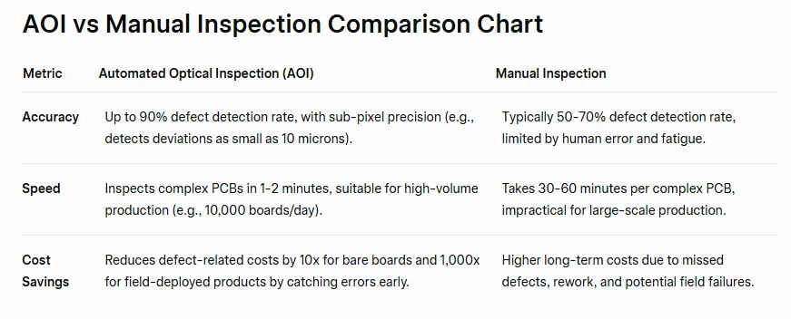
AOI systems achieve sub-pixel accuracy, detecting defects that the human eye cannot. For instance, a study in the 'International Journal of Engineering and Advanced Technology' found that AOI reduces defect escape rates by up to 90% compared to manual inspection. This precision is critical for high-reliability applications like aerospace, where a single solder bridge could disrupt signal integrity at 5 GHz.
2. Increased Efficiency
Manual inspection of a complex PCB can take 30–60 minutes, while AOI completes the same task in 1–2 minutes. This speed is essential for high-volume production, where thousands of boards are assembled daily. By catching defects early, AOI also minimizes rework, saving time and materials.
3. Cost Savings
Early defect detection reduces the cost of errors exponentially. The same study noted that fixing a defect in a bare board costs 10 times less than in an assembled board, and 1,000 times less than in a field-deployed product. AOI's ability to identify issues before they escalate translates to significant savings.
4. Flexibility Across Production Stages
AOI can be applied to bare PCBs, post-solder paste application, or fully assembled boards. For example, it verifies trace widths (e.g., ensuring 0.1 mm traces meet ±10% tolerance) during fabrication and checks component polarity during assembly. This versatility makes AOI adaptable to diverse manufacturing needs.
5. Improved Process Control
AOI provides actionable data to refine manufacturing processes. If an AOI system detects repeated solder voids, engineers can adjust reflow oven temperatures (e.g., increasing peak temperature from 245°C to 250°C) to improve outcomes.
Common Defects Detected by AOI
AOI excels at identifying a wide range of surface-level defects, including:
- Solder Joint Issues: Insufficient solder (e.g., <50% pad coverage), excessive solder, or solder bridges causing shorts.
- Component Placement Errors: Missing components, misaligned parts (e.g., a capacitor offset by 0.2 mm), or incorrect polarity.
- PCB Fabrication Flaws: Scratches, open circuits, or trace width violations (e.g., a 0.15 mm trace reduced to 0.12 mm).
- Surface Imperfections: Stains, nodules, or excess copper affecting signal integrity.
- Component Marking Errors: Incorrect or unreadable markings, such as a resistor mislabeled as 10 kΩ instead of 100 kΩ.
While AOI is highly effective for surface defects, it cannot inspect internal layers or hidden solder joints (e.g., under BGA packages). In such cases, complementary methods like Automated X-ray Inspection (AXI) are used, though AXI is costlier due to its complex setup.
Limitations of AOI and How to Address Them
Despite its strengths, AOI has limitations that engineers must consider:
1. Surface-Only Inspection
AOI cannot detect internal defects, such as voids in multi-layer PCBs. Solution: Pair AOI with AXI or in-circuit testing for comprehensive quality control.
2. False Positives
AOI may flag acceptable variations (e.g., a slightly oversized solder joint) as defects, slowing production. Solution: Fine-tune algorithms and train operators to distinguish false positives, reducing false call rates by up to 30%.
3. Complex Setup
Programming AOI systems for new PCB designs can be time-intensive. Solution: Use AI-assisted programming, as seen in modern systems like Mycronic's MYPro I series, to streamline setup.
4. Component Shadowing
Tall components may block light, obscuring shorter ones. Solution: Employ multi-angle lighting and 3D AOI systems to capture obscured areas.
By understanding these limitations and implementing complementary strategies, manufacturers can maximize AOI's effectiveness.
Suggested Reading:AOI to the Rescue: Detecting and Preventing Component Misplacement on PCBs
The Future of AOI in PCB Assembly
As PCBs become smaller and more complex, AOI technology continues to evolve. Emerging trends include:
- 3D AOI Systems: These provide volumetric data, measuring solder joint height and component coplanarity with precision (e.g., detecting deviations as small as 5 microns).
- AI and Machine Learning: AI-driven AOI systems, like those using transfer learning, improve defect detection accuracy by learning from past inspections, reducing false positives by up to 20%.
- Integration with Industry 4.0: AOI systems are increasingly connected to smart factories, enabling real-time data sharing and predictive maintenance. For example, AOI data can trigger automatic adjustments in solder paste printers, maintaining 95% yield rates.
- High-Speed Processing: Advances in GPU technology allow AOI systems to process images at 100 frames per second, keeping pace with high-throughput lines producing 10,000 boards daily.
These innovations ensure that AOI remains a critical tool for meeting the demands of modern electronics manufacturing.
How ALLPCB Supports Quality PCB Assembly with AOI
At ALLPCB, we prioritize delivering high-quality PCBs to meet the needs of engineers worldwide. Our advanced manufacturing facilities integrate state-of-the-art AOI systems to ensure every board meets exacting standards. With quick-turn prototyping, we can deliver fully inspected PCBs in as little as 24 hours, while our global logistics ensure timely delivery for high-volume production. By combining AOI with other quality control methods like AXI and functional testing, we provide reliable, defect-free boards for applications ranging from consumer electronics to aerospace. Our commitment to precision and efficiency empowers engineers to bring their designs to market with confidence.
Conclusion
Automated Optical Inspection is a game-changer in PCB assembly, offering unmatched accuracy, efficiency, and cost savings. By detecting defects early and providing actionable data, AOI ensures that PCBs meet the high standards required for today's complex electronics. As technology advances, AOI continues to evolve, incorporating 3D imaging, AI, and smart factory integration to stay ahead of industry demands. For engineers, understanding and leveraging AOI is key to delivering reliable, high-performance products. At ALLPCB, we're proud to harness this technology to support your next project, ensuring quality at every step.


