 ALLPCB


What Is PCB Via Failure Analysis and Why It Matters
PCB via failure analysis examines the physical and electrical conditions that cause vias to stop functioning correctly. The process identifies defects such as plating voids, barrel cracks, or poor hole-wall adhesion that develop during fabrication or operation. Industry professionals apply this analysis when boards exhibit unexpected resistance changes or open circuits after environmental stress. Reliable via performance directly influences product longevity in automotive, aerospace, and consumer electronics sectors. Early detection prevents costly field returns and supports consistent manufacturing yields.
Technical Principles and Common Causes of Via Failures
Vias consist of a drilled hole lined with electroplated copper that links copper layers on a multilayer board. Thermal expansion mismatch between the copper barrel and surrounding laminate creates mechanical stress during temperature changes. Repeated cycling can initiate microcracks that propagate through the plating and interrupt current flow. Manufacturing variations such as insufficient copper thickness or incomplete hole cleaning also contribute to early failures. Engineers evaluate these factors by correlating board design parameters with observed failure locations.
Plating quality inside the via barrel determines long-term electrical continuity. Thin or uneven deposits leave voids that act as stress concentrators under load. Resin smear remaining after drilling prevents proper adhesion and promotes delamination over time. High-aspect-ratio vias in thick boards increase the difficulty of achieving uniform plating coverage. These physical characteristics explain why failures often appear first in boards subjected to reflow soldering or power cycling.
Related Reading: Different PCB Hole Types, Thru hole, Blind vias, Buried vias
Methods for Conducting PCB Via Failure Analysis
Visual inspection serves as the initial step in PCB via failure analysis because surface anomalies often indicate deeper problems. Magnification reveals discoloration, lifted pads, or visible cracks around via openings. This non-destructive approach quickly narrows the focus before more advanced techniques are applied. Engineers document findings with photographs to track progression during subsequent tests.
X-ray inspection provides internal visibility into via structures without sectioning the board. It highlights voids, barrel thinning, and misregistration between layers that optical methods cannot detect. High-resolution images allow measurement of copper thickness and identification of plating gaps. Teams use this technique on production samples to verify process consistency before full-scale assembly.
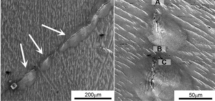
SEM analysis delivers high-magnification images of via cross-sections after careful preparation. It exposes grain structure in the copper plating and detects micro-cracks invisible to standard optical microscopes. Energy-dispersive spectroscopy can further characterize contaminants or oxide layers at failure sites. This level of detail supports precise root cause determination when electrical data alone remains inconclusive.
Electrical testing quantifies via performance through resistance measurements and continuity checks across temperature ranges. Four-point probe methods isolate via resistance from trace contributions and reveal intermittent opens under thermal load. Burn-in testing accelerates aging to expose latent defects before boards reach customers. Results from these tests guide decisions on whether a failure stems from design, material, or process issues.
Root cause analysis integrates data from all prior steps to establish the sequence of events leading to failure. Engineers map failure locations against design files and process records to identify patterns. Statistical review of multiple samples distinguishes random defects from systemic problems. This structured approach ensures corrective actions address the true origin rather than symptoms.

Best Practices to Prevent and Mitigate Via Failures
Design rules that limit via aspect ratios and specify minimum copper thickness reduce mechanical stress concentrations. Specifying IPC-6012E requirements for rigid boards during procurement helps ensure plating meets established performance thresholds. Controlled impedance calculations and proper via placement away from high-stress board regions further improve reliability. These choices occur early in the layout phase and influence every subsequent manufacturing step.
Process controls during drilling and plating directly affect via integrity. Clean hole walls free of resin smear promote uniform copper deposition.
Monitoring plating bath chemistry and current density maintains consistent barrel thickness across production lots. Post-plating thermal stress relief cycles can stabilize the structure before final assembly. Consistent application of these controls lowers the incidence of latent defects.
Related Reading: Troubleshooting Blind Via Failures: A Practical Guide for PCB Engineers
Conclusion
Effective PCB via failure analysis combines visual inspection, x-ray inspection, SEM analysis, electrical testing, and root cause analysis into a coherent workflow. Each technique reveals different aspects of via condition and together they provide a complete picture of failure mechanisms. Adherence to recognized standards such as IPC-A-600K supports consistent evaluation criteria across teams. Implementing the practices outlined here helps engineers maintain board reliability throughout product life cycles.
FAQs
Q1: What steps are involved in PCB via failure analysis?
A1: PCB via failure analysis typically begins with visual inspection followed by x-ray inspection and SEM analysis to locate physical defects. Electrical testing then confirms functional impact, after which root cause analysis identifies whether design, material, or process factors are responsible. This sequence ensures thorough diagnosis without overlooking contributing variables.
Q2: How does x-ray inspection support PCB via failure analysis?
A2: X-ray inspection allows engineers to examine via barrels and plating thickness inside multilayer boards without destructive sectioning. It detects voids, cracks, and registration errors that affect electrical continuity. Results from x-ray inspection guide decisions on whether further SEM analysis or electrical testing is required.
Q3: Why is root cause analysis important after electrical testing of vias?
A3: Root cause analysis connects electrical test results with physical evidence gathered through visual inspection and SEM analysis. It distinguishes between isolated manufacturing defects and recurring design or process issues. This step enables targeted corrective actions that improve future board reliability.
Q4: When should SEM analysis be used in PCB via failure analysis?
A4: SEM analysis is applied when visual inspection and x-ray inspection indicate possible microcracks or plating irregularities but cannot provide sufficient detail. It reveals grain structure and contamination at high magnification. Engineers typically reserve SEM analysis for critical failures where precise mechanism identification is necessary.
References
IPC-6012E — Qualification and Performance Specification for Rigid Printed Boards. IPC, 2017
IPC-A-600K — Acceptability of Printed Boards. IPC, 2020
JEDEC J-STD-020E — Moisture/Reflow Sensitivity Classification. JEDEC, 2014





