 ALLPCB


Introduction
Blind vias play a crucial role in high-density interconnect (HDI) printed circuit boards, enabling compact designs by connecting surface layers to specific inner layers without penetrating the entire board thickness. These structures allow for increased routing density and improved signal integrity in modern electronics, but they are prone to failures that can lead to open circuits, intermittent connectivity, or complete board rejection. PCB engineers often encounter blind via issues during manufacturing qualification, reliability testing, or field returns, making effective troubleshooting essential for maintaining product quality and reducing costs. This guide focuses on blind via failure analysis, common blind via defects, blind via testing methods, and blind via repair techniques, providing structured insights tailored for electrical engineers. By understanding the root causes and systematic approaches to diagnosis, engineers can implement preventive measures aligned with industry standards. The following sections break down the mechanisms, detection strategies, and remediation steps to help resolve these challenges efficiently.
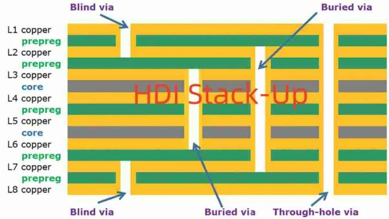
What Are Blind Vias and Why Do They Matter?
Blind vias are plated-through holes that originate from one surface of the PCB and terminate at an inner layer, distinguishing them from through vias that span the full board height. In HDI PCBs, they facilitate layer-to-layer interconnections in multilayer stacks, supporting finer pitch components and higher I/O counts essential for applications like smartphones and automotive electronics. Their implementation requires precise sequential lamination and drilling processes, often using laser or controlled-depth mechanical methods to achieve accurate depth control. Failures in blind vias matter because they compromise electrical performance, leading to yield losses during production or reliability failures under thermal cycling. Engineers must prioritize blind via integrity to meet performance specifications in dense designs. Without robust blind vias, overall board reliability diminishes, impacting signal paths and power distribution networks.
The relevance of blind vias grows with the demand for miniaturization, where traditional through vias would consume excessive space and introduce unwanted stubs affecting high-speed signals. Proper design and fabrication ensure minimal inductance and capacitance, preserving signal integrity. However, their partial depth makes them susceptible to process variations not seen in full through holes. Addressing blind via failures early in the design verification phase prevents costly respins. Factory-driven insights emphasize adherence to qualification criteria for these features.
Common Blind Via Defects
Common blind via defects arise primarily from plating inconsistencies, mechanical stresses, and process misalignments during fabrication. Plating voids or incomplete copper deposition within the via barrel often result from inadequate electroplating parameters, leading to high-resistance paths or open circuits. Cracking in the copper barrel frequently occurs due to thermal fatigue, where coefficient of thermal expansion (CTE) mismatches between copper plating and dielectric materials induce stress during reflow or operational temperature swings. These cracks propagate under cyclic loading, manifesting as intermittent failures in field use.
Another prevalent issue is empty caves or dimples in copper-filled blind vias, caused by gas entrapment or improper filling during plating, which weakens structural integrity and promotes corrosion. Poor via bottom metallization, where the landing pad lacks sufficient copper coverage, results from drill smear residue or etch-back deficiencies. Misregistration between layers during lamination can cause the via to miss its target pad entirely, creating non-contact opens. Delamination at the via-dielectric interface may stem from inadequate adhesion promotion or moisture absorption prior to lamination.
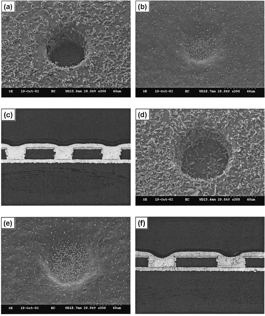
These defects not only fail electrical continuity tests but also accelerate under environmental stresses like humidity and vibration. Identifying them requires correlating manufacturing data with failure signatures. Engineers should review drill depth logs and plating bath analytics to pinpoint origins.
Mechanisms Behind Blind Via Failures
Blind via failures stem from interconnected mechanisms involving drilling precision, plating chemistry, and material interactions. During laser or mechanical drilling, excessive energy or misalignment can create tapered holes with uneven walls, complicating uniform plating and leading to thin spots prone to electromigration. Plating processes must achieve minimum thickness per IPC-6012DS specifications to withstand current densities without void formation. Inadequate desmear or activation results in poor adhesion, fostering voids that expand under thermal expansion.
Thermal-mechanical stresses dominate reliability failures, as blind vias experience higher localized strains due to their shallower depth and proximity to surface features. CTE differentials cause barrel cracking, especially in stacked via configurations where cumulative stresses amplify. Aspect ratio exceeding recommended limits hampers electrolyte penetration, promoting nonuniform deposition and weak bottoms.
Material selection influences defect susceptibility; low-loss dielectrics with mismatched Tg can delaminate under solder reflow. Process-induced warpage from asymmetric lamination further misaligns vias. Understanding these mechanisms guides targeted blind via failure analysis.
Blind Via Testing Methods
Blind via testing methods combine nondestructive and destructive techniques to verify continuity, plating quality, and structural integrity. Electrical testing via flying probe or bed-of-nails fixtures detects opens and shorts at high resolution, suitable for production nets including blind vias. Time-domain reflectometry (TDR) quantifies impedance discontinuities from plating defects or cracks, aiding signal integrity correlation.
Nondestructive options include X-ray laminography for visualizing internal via fill and bottom coverage without sectioning. Scanning acoustic microscopy (SAM) identifies delaminations and voids by ultrasonic wave reflections at interfaces. Dye penetrant testing reveals microcracks by capillary action into flaws.
Destructive cross-sectioning provides definitive analysis: polish to via center, etch, and inspect under optical or SEM for plating thickness, voids, and cracks per IPC-A-600 acceptability criteria. These methods form a tiered approach, starting with electrical nets and escalating to microscopy for root cause.
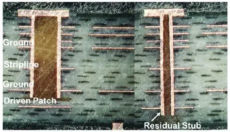
Combining methods accelerates diagnosis; for instance, X-ray flags suspects before sectioning. Engineers should document test conditions to trace process excursions.
Blind Via Failure Analysis Workflow
A systematic blind via failure analysis begins with failure mode confirmation through continuity mapping and thermal cycling to replicate conditions. Review design files against fabrication drawings for aspect ratio, depth specs, and pad sizing compliance. Correlate with process data like drill charts and plating coupons.
Nondestructive imaging prioritizes: 2D/3D X-ray for misalignment, SAM for subsurface voids. If inconclusive, targeted cross-sections at failure sites quantify plating metrics. Fractography on cracked samples reveals stress origins, distinguishing fatigue from overload.
Root cause verification involves controlled simulations, such as accelerated thermal cycling per JEDEC standards, to confirm mechanisms. Report findings with micrographs and recommendations, closing the loop on prevention.
This workflow minimizes board consumption while maximizing insights for design iterations.
Blind Via Repair Techniques
Blind via repair techniques are limited due to their embedded nature, often favoring prevention over fixes, but viable options exist for prototypes or low-volume boards. For open circuits from minor plating defects, z-axis conductive epoxy filling restores conductivity after via cleaning and inspection. Apply epoxy via syringe, cure per manufacturer specs, and verify continuity without exceeding current ratings.
Cracked barrels may require partial backdrilling to remove damaged sections, followed by conductive fill, though this risks adjacent features. Laser ablation for precise stub removal precedes replating in advanced facilities, but demands cleanroom conditions.
Surface-level repairs like jumper wires suit accessible outer-layer connections, soldered and insulated per assembly standards. However, repairs compromise reliability for high-volume production, prompting redesigns with larger margins or buried alternatives.
Success hinges on failure scope; extensive defects necessitate board replacement. Document repairs for traceability.
Best Practices for Prevention
Prevent blind via defects through design rules like aspect ratios under 1:1, generous annular rings, and staggered via placement to mitigate stress. Specify plating per IPC-6012DS, mandating minimum copper thickness and fill verification. Collaborate on process controls: optimized laser parameters, robust desmear, and pulse plating for uniformity.
Material selection favors low-CTE cores with matched builds to curb warpage. Qualification via thermal cycling and MSL testing uncovers latent issues early. In-line monitoring with automated X-ray ensures compliance.
These practices align factory capabilities with engineering needs, boosting yields.
Troubleshooting Case Insights
In a typical scenario, batch opens traced to blind vias revealed cracking via cross-section, linked to high aspect ratios and reflow profiles. Adjusting design to 0.8:1 ratio and slowing ramp rates resolved recurrence. Another case involved voids from gas in plating; bath agitation improvements and vacuum filling eliminated them.
These highlight iterative analysis's value.
Conclusion
Troubleshooting blind via failures demands a blend of precise testing, methodical analysis, and proactive design. By mastering common defects like cracking and voids, engineers can deploy effective blind via testing methods and selective repairs. Adhering to standards ensures reliability in HDI applications. Implement these strategies to enhance PCB robustness and streamline production.
FAQs
Q1: What are the most common blind via defects encountered in PCB manufacturing?
A1: Common blind via defects include plating voids, barrel cracking from thermal stress, empty caves in filled vias, and misregistration leading to poor bottom contact. These arise from plating inconsistencies, CTE mismatches, and drilling inaccuracies. Early detection via electrical testing and X-ray prevents yield impacts. Factory process tweaks like improved desmear address root causes effectively.
Q2: How do you perform blind via failure analysis step-by-step?
A2: Start with electrical continuity tests to isolate nets, followed by nondestructive X-ray or SAM for internal views. Cross-section suspects for microscopic plating inspection. Correlate with process data and simulate stresses. This tiered approach pinpoints mechanisms like cracks or voids systematically.
Q3: What blind via testing methods are best for production quality control?
A3: Flying probe electrical testing verifies connectivity, while X-ray laminography checks fill and alignment. SAM detects delaminations nondestructively. Combine with TDR for signal issues. These ensure compliance without excessive handling.
Q4: Are there reliable blind via repair techniques for failed boards?
A4: Conductive epoxy fill repairs minor opens after cleaning, verified by continuity tests. Backdrilling suits deeper cracks, but limits apply. Prevention via design rules outperforms repairs for production reliability.
References
IPC-6012DS — Qualification and Performance Specification for High Density Interconnect (HDI) Printed Boards. IPC, 2017
IPC-A-600K — Acceptability of Printed Boards. IPC, 2020





