 ALLPCB


VR Headset PCB Prototyping: Fast and Cost-Effective Methods
Introduction
Virtual reality headsets demand compact, high-performance printed circuit boards that handle high-speed data transmission, precise sensor integration, and efficient power distribution within tight spatial constraints. Engineers working on these devices must balance performance requirements with the need for rapid iteration during development cycles. PCB prototyping serves as a critical step that allows validation of designs before committing to volume production. Effective prototyping methods reduce development time while controlling expenses associated with multiple design revisions. This approach supports the creation of reliable hardware that meets the demanding operational conditions typical of immersive display systems.
Why VR Headset PCB Prototyping Matters
Prototyping enables engineers to test electrical performance, thermal behavior, and mechanical fit within the limited enclosure of a VR headset. Early identification of issues such as signal integrity problems or excessive heat generation prevents costly changes later in the project. The process also supports evaluation of component placement strategies that influence overall device weight and user comfort. Procurement teams benefit from accurate cost estimates derived from prototype runs, which inform budgeting for subsequent stages. In an industry driven by rapid technological advancement, timely prototyping helps maintain competitive development schedules without compromising quality standards.
Technical Principles of PCB Prototyping for VR Applications
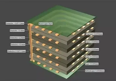
High-density interconnect technology forms the foundation for VR headset boards, allowing multiple layers to route complex signals while maintaining controlled impedance. Engineers apply stack-up planning to manage crosstalk and electromagnetic interference between high-speed interfaces and power planes. Thermal vias and copper pours distribute heat from processors and display drivers, following principles outlined in relevant industry specifications for thermal management. Material selection focuses on substrates with appropriate glass transition temperatures and low dielectric constants to support stable operation across temperature variations encountered during extended use. Signal integrity analysis during the prototyping phase verifies that trace geometries and via placements meet performance targets before physical fabrication begins.
Fast and Cost-Effective Prototyping Methods
Rapid PCB fabrication services utilize advanced imaging and etching processes that deliver functional boards in days rather than weeks. Panelization techniques optimize material usage by combining multiple prototype designs on a single panel, lowering per-unit costs during initial runs. Engineers often select standard laminate materials and common copper weights to avoid premium pricing associated with specialized substrates. Quick-turn assembly incorporates automated placement equipment that handles fine-pitch components typical in VR designs, reducing manual labor expenses. Iterative testing after each prototype cycle provides data that guides targeted modifications, minimizing the total number of fabrication iterations required.
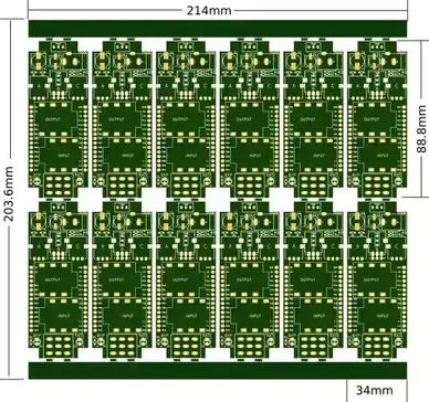
Design for manufacturability reviews conducted early in the process identify potential issues such as insufficient solder mask clearance or via-in-pad requirements. These reviews streamline the transition from prototype to production by aligning layout choices with standard fabrication capabilities. Flexible and rigid-flex constructions, when needed for folding display assemblies, follow established guidelines that ensure reliable bending performance without excessive material waste. Cost modeling during prototyping compares different via structures and layer counts to identify configurations that deliver required functionality at the lowest expense.
Best Practices in Assembly and Quality Verification
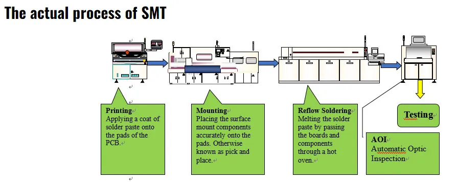
Surface-mount technology assembly for VR prototypes emphasizes precise stencil design and reflow profiling to achieve consistent solder joints on miniature components. Engineers monitor warpage during thermal cycling to maintain alignment between packages and pads, using measurement techniques consistent with established acceptability criteria. Electrical testing includes continuity checks, insulation resistance measurements, and functional validation of sensor interfaces before full system integration. Documentation of each prototype revision supports traceability and accelerates troubleshooting when performance deviations appear.
Adherence to IPC-A-600 guidelines during incoming inspection helps verify that fabricated boards meet visual and dimensional requirements before assembly proceeds. This practice reduces the risk of incorporating defective material into functional prototypes. Thermal profiling during reflow follows principles from J-STD-020 to classify component moisture sensitivity and prevent damage during processing.
Conclusion
Effective VR headset PCB prototyping combines rapid fabrication techniques with disciplined design practices to deliver functional boards quickly and economically. Structured approaches to stack-up planning, material selection, and assembly verification support reliable performance validation. By focusing on manufacturability and targeted testing, engineering teams achieve shorter development cycles while controlling overall project costs. These methods ultimately contribute to the production of compact, high-performance devices that meet user expectations for immersive experiences.
FAQs
Q1: What factors influence the cost of VR headset PCB prototyping?
A1: Board complexity, layer count, material choices, and assembly requirements primarily determine expenses. Engineers optimize designs for standard processes and panel utilization to achieve lower per-unit costs during prototype runs. Accurate cost modeling early in development helps align expectations with available budgets while maintaining necessary performance levels.
Q2: How does rapid PCB prototyping benefit VR headset development timelines?
A2: Fast fabrication and assembly cycles allow multiple design iterations within compressed schedules typical of consumer electronics projects. Early validation of electrical and thermal characteristics reduces the likelihood of major revisions after initial hardware testing. This approach supports parallel work on firmware and mechanical integration without extended delays.
Q3: What role does quality verification play in prototype assembly for VR applications?
A3: Systematic inspection and electrical testing confirm that assembled boards meet functional requirements before integration into headset enclosures. Following established acceptability standards during this phase minimizes the introduction of defects that could affect device reliability or user safety. Documentation from verification steps provides valuable data for subsequent design refinements.
Q4: Which standards guide material and process decisions in VR PCB prototyping?
A4: Specifications such as IPC-6012 establish performance requirements for rigid boards used in demanding applications. Additional guidance from J-STD-020 supports proper handling of moisture-sensitive components during reflow assembly. These references help ensure consistent quality across prototype builds without introducing unnecessary process variations.
References
IPC-6012E — Qualification and Performance Specification for Rigid Printed Boards. IPC, 2017
IPC-A-600K — Acceptability of Printed Boards. IPC, 2020
JEDEC J-STD-020E — Moisture/Reflow Sensitivity Classification. JEDEC, 2014





