 ALLPCB


Three-dimensional printed circuit boards extend traditional flat layouts into non-planar geometries. Engineers can position conductive traces and components along curved or multi-axis surfaces. This approach supports compact product enclosures while preserving electrical performance. Design teams gain freedom to integrate mechanical housings directly with circuitry. The result is reduced overall volume and simplified assembly sequences in many applications.
What 3D PCBs Are and Why They Matter
A 3D PCB consists of a substrate formed or printed into three-dimensional shapes rather than remaining strictly planar. Conductive paths follow the contours of the structure, and components mount on multiple faces or angled planes. This configuration differs from conventional rigid boards that occupy a single flat layer stack. The technology draws on additive processes or molded interconnect devices to achieve the required geometry.
The approach addresses persistent constraints in electronics packaging. Space-limited devices such as wearables, automotive sensors, and aerospace modules benefit from the ability to conform circuitry to available volume. Weight savings arise when separate mechanical brackets become unnecessary. Thermal paths can also be optimized by placing heat-generating parts closer to cooling surfaces. These characteristics explain growing interest among electric engineers who must balance electrical, mechanical, and thermal requirements within shrinking envelopes.
Technical Principles of 3D PCB Construction
The core mechanism involves creating a three-dimensional dielectric base and then depositing or embedding conductive material along its surfaces. Traces may run across curved sections or transition between planes without traditional vias in every location. Component attachment occurs through surface-mount techniques adapted for non-horizontal orientations. Electrical continuity is maintained by controlling trace width, spacing, and material properties to match impedance and current-carrying needs.
Manufacturing sequences typically begin with substrate formation, followed by patterning of conductors. Subsequent steps include dielectric layering where required and final component placement. Thermal expansion coefficients must remain compatible across materials to limit stress during temperature cycling. Warpage control becomes critical because deviations from intended geometry can affect both mechanical fit and electrical performance.
Related Reading: 3D PCB Printing for Aerospace: A New Dimension in Circuitry
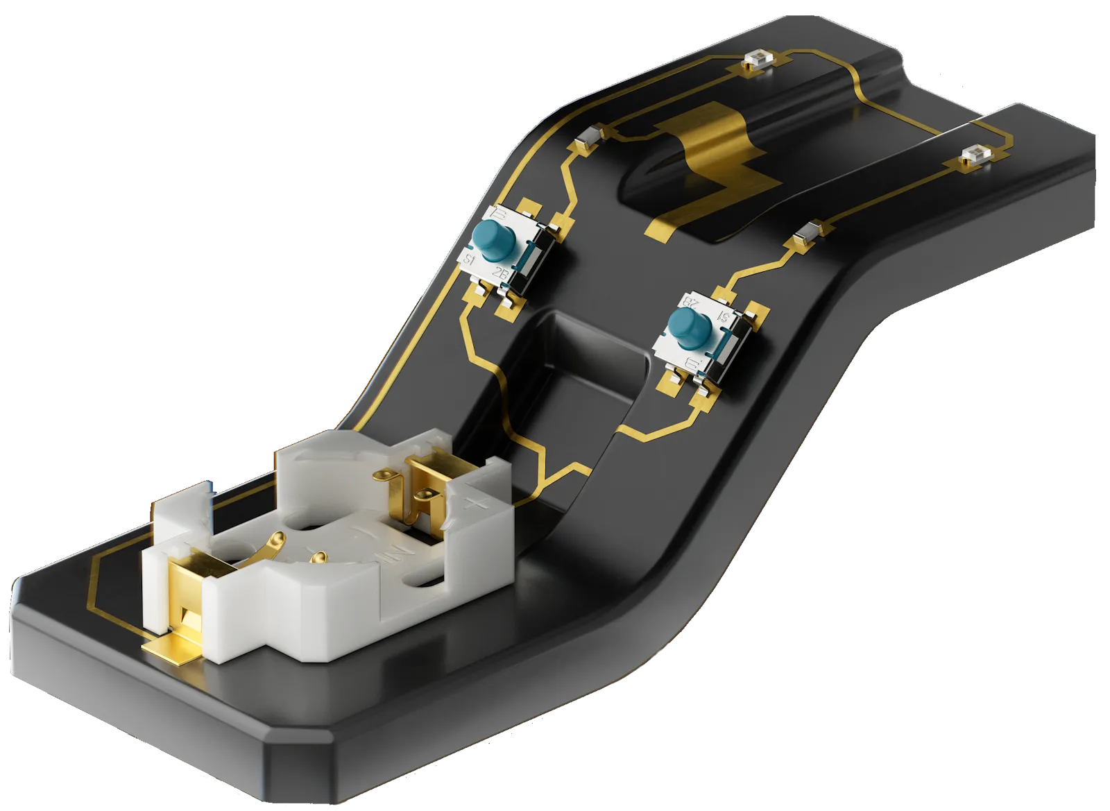
Engineers evaluate signal integrity by modeling trace lengths and return paths in the three-dimensional layout. Power distribution networks require careful routing to avoid voltage drops across extended paths. Electromagnetic compatibility considerations include shielding effectiveness when traces occupy multiple orientations relative to potential noise sources.
Design Flexibility and Manufacturing Advantages
3D PCB design flexibility allows placement of components on surfaces that would otherwise remain unused. Enclosures can incorporate circuitry directly, eliminating separate interconnects such as cables or flex circuits in some cases. This integration reduces part count and potential failure points. Assembly processes benefit when pick-and-place operations occur on a single formed structure rather than multiple flat boards.
Manufacturing advantages include shorter interconnect distances that can lower resistive losses. The ability to follow product contours often improves airflow or heat sinking without additional hardware. Production yields depend on process control of substrate forming and conductor deposition steps. When these parameters are managed within established tolerances, the resulting assemblies demonstrate consistent electrical characteristics across production lots.
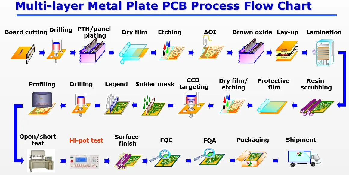
Design rules adapt from planar standards to account for draft angles, minimum bend radii, and material flow during forming. Trace routing must consider line-of-sight requirements for certain deposition methods. Thermal vias or embedded heat spreaders may be incorporated to manage localized heating on vertical or angled surfaces.
Related Reading: Multi-Layer PCB Manufacturing: A Deep Dive into the Production Process
Addressing 3D PCB Design Limitations
3D PCB design limitations center on process complexity and material constraints. Substrate materials must withstand forming operations without cracking while maintaining dielectric strength. Conductor adhesion on curved surfaces requires surface preparation techniques that differ from flat-board processing. Inspection of internal features becomes more involved when geometries obstruct direct visual or probe access.
Cost considerations arise from specialized tooling and lower throughput compared with high-volume planar production. Rework options are restricted once components are attached to non-planar surfaces. Qualification testing follows the same environmental and electrical stress sequences used for conventional boards, yet sample preparation and fixturing demand additional engineering effort.
Electric engineers mitigate these limitations through iterative simulation of mechanical and thermal behavior before committing to physical prototypes. Material selection prioritizes compatibility with both forming and soldering temperatures. Design reviews incorporate feedback from manufacturing partners on achievable tolerances for specific geometries.
Best Practices for Implementation
Successful projects begin with clear definition of mechanical envelope and electrical interface requirements. Early collaboration between electrical and mechanical teams identifies opportunities for functional integration. Simulation tools evaluate signal integrity, thermal profiles, and mechanical stress prior to layout finalization. Prototype iterations focus on validating forming accuracy and trace continuity rather than full functional testing in initial builds.
Process documentation should reference applicable industry standards for board construction and acceptance criteria. IPC-6012E provides qualification and performance requirements for rigid printed boards that serve as a baseline for many 3D constructions. IPC-A-600K outlines acceptability criteria that guide visual and dimensional inspection regardless of final geometry.
Procurement specifications include material certifications and process capability data. Incoming inspection verifies substrate dimensions and surface finish before patterning. Assembly documentation details orientation-specific handling to prevent damage during component placement and reflow.
Conclusion
3D PCBs expand the solution space available to electric engineers by allowing circuitry to occupy three-dimensional volumes. The resulting design flexibility supports more compact and integrated products while introducing manageable manufacturing considerations. When projects follow structured design practices and reference established standards such as those from IPC, the technology delivers reliable performance in demanding applications. Continued refinement of materials and processes is expected to broaden adoption across additional market segments.
FAQs
Q1: What are the primary 3D PCB design benefits compared with traditional flat boards?
A1: Three-dimensional PCBs enable components and traces to occupy multiple planes and curved surfaces within a single structure. This configuration reduces overall product volume and eliminates some interconnect hardware. Engineers achieve tighter integration of electrical and mechanical functions while maintaining required electrical performance when design rules are applied correctly.
Q2: How does 3D PCB design flexibility affect product development cycles?
A2: The added freedom allows mechanical and electrical teams to iterate enclosure shapes and circuit layouts in parallel. Early simulation identifies geometric constraints before tooling investment. Resulting prototypes often require fewer revisions because functional and packaging requirements are addressed simultaneously from the start.
Q3: What manufacturing advantages does 3D PCB technology offer in high-reliability sectors?
A3: Shorter interconnect paths and integrated mechanical features can improve vibration resistance and reduce weight. When process controls align with standards such as IPC-6012E, consistent electrical characteristics are achievable across production volumes. These factors support applications where size, weight, and reliability are critical constraints.
Q4: What are the main 3D PCB design limitations that engineers must evaluate?
A4: Forming processes introduce constraints on minimum bend radii and material compatibility. Inspection access and rework options are more limited than on planar boards. Thermal and mechanical modeling must account for three-dimensional stress distributions to ensure long-term reliability under expected operating conditions.
References
IPC-6012E — Qualification and Performance Specification for Rigid Printed Boards. IPC, 2017
IPC-A-600K — Acceptability of Printed Boards. IPC, 2020
JEDEC J-STD-020E — Moisture/Reflow Sensitivity Classification. JEDEC, 2014





