 ALLPCB


Aluminum PCBs serve as essential substrates in applications requiring efficient heat dissipation, such as power electronics and LED systems. Their metal core construction introduces unique challenges during validation, making comprehensive testing indispensable for ensuring long-term functionality. Engineers rely on systematic evaluation to verify both electrical integrity and thermal performance under operational stresses. This approach helps identify potential weaknesses early in the development cycle, reducing the risk of field failures. Structured testing protocols align with established industry practices to maintain consistency across production batches.
Why Advanced Testing Matters for Aluminum PCBs
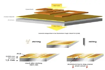
Aluminum PCBs differ from traditional FR4 boards due to their enhanced thermal conductivity, which demands specialized verification methods. Without rigorous assessment, issues like delamination or uneven heat spreading can compromise device reliability in demanding environments. Procurement teams and designers benefit from understanding these requirements to specify appropriate validation steps during sourcing. Effective testing supports compliance with performance expectations in sectors ranging from automotive to industrial controls. It also facilitates iterative improvements in board design by providing quantifiable data on material behavior.
Technical Principles of Aluminum PCB Testing
Electrical testing focuses on continuity and insulation resistance to confirm that conductive paths remain intact after lamination and etching processes. These checks detect micro-cracks or voids that might arise from the mechanical stresses of bonding aluminum to dielectric layers. Thermal testing evaluates heat transfer efficiency and measures parameters such as thermal resistance through controlled temperature gradients. Warpage assessment quantifies dimensional stability under thermal cycling, which is critical because aluminum expands differently from copper traces and insulating materials. Environmental testing simulates humidity, vibration, and temperature extremes to predict long-term degradation mechanisms.
Reliability testing integrates accelerated life simulations to model real-world usage patterns without introducing artificial assumptions. Engineers structure these evaluations sequentially, beginning with baseline measurements and progressing to stress conditions that reveal cumulative effects. This logical progression ensures that each test builds upon prior results for comprehensive characterization. Data from these procedures guide adjustments in layer stack-up or via placement to optimize overall board performance.
Practical Solutions and Best Practices
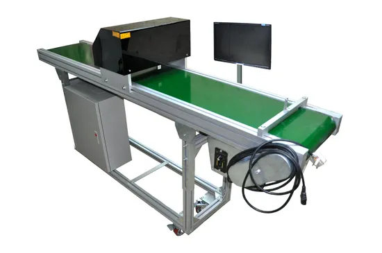
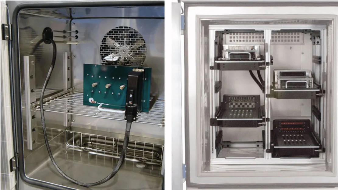
Implementing PCB electrical testing involves four-point probe techniques for precise resistance mapping across the circuit. Technicians perform these measurements at multiple stages, including after etching and final assembly, to isolate process-related defects. For PCB thermal testing, engineers apply steady-state heat flow methods that quantify conductivity while accounting for interface resistances at the metal core. Best practices recommend calibrating equipment regularly and documenting environmental conditions during each run to ensure repeatability. PCB reliability testing often incorporates thermal shock cycles that alternate between high and low temperatures, allowing observation of crack propagation at solder joints or dielectric interfaces.
PCB environmental testing extends these efforts by exposing boards to controlled humidity chambers and mechanical vibration tables. Teams analyze failure modes through post-test microscopy and electrical re-verification to correlate observed changes with specific stress factors. Structured documentation of test sequences supports traceability and enables comparison across design revisions. This methodical framework helps teams prioritize modifications that enhance durability without unnecessary over-engineering.
Related Reading: The Ultimate Guide to PCB Inspection: Techniques and Technologies
Reliability Insights for High-Performance Applications
In high-power scenarios, combining PCB thermal testing with reliability protocols reveals how aluminum substrates maintain performance after prolonged exposure to elevated temperatures. Engineers examine parameters such as dielectric breakdown voltage following environmental conditioning to confirm insulation integrity remains within acceptable limits. Practical troubleshooting often centers on identifying localized hot spots through infrared imaging, which guides refinements in copper pour distribution. These insights foster designs that balance thermal efficiency with mechanical robustness across varying load conditions.
Related Reading: PCB Reliability Testing: Uncovering Hidden Weaknesses with Accelerated Thermal Cycling
Conclusion
Advanced testing methods for aluminum PCBs provide engineers with the data needed to validate designs against operational demands. By integrating electrical, thermal, reliability, and environmental evaluations, teams achieve consistent quality while addressing the distinct characteristics of metal-core constructions. Adherence to logical testing sequences supports informed decision-making throughout the product lifecycle. Ultimately, these practices contribute to more dependable electronic systems in thermally challenging applications.
FAQs
Q1: What role does aluminum PCB testing play in ensuring product reliability?
A1: Aluminum PCB testing verifies electrical continuity, thermal conductivity, and mechanical stability to confirm boards perform as intended under load. Systematic evaluation identifies defects early, supporting consistent outcomes in power and lighting applications. Engineers use these results to refine layouts and material selections for improved longevity.
Q2: How does PCB electrical testing differ for aluminum substrates compared to standard boards?
A2: PCB electrical testing on aluminum substrates accounts for the metal core's influence on current distribution and insulation properties. Technicians apply specialized probe methods to detect issues arising from lamination stresses. This ensures signal integrity remains high despite the enhanced heat-spreading capabilities.
Q3: Why is PCB thermal testing essential for aluminum PCBs in high-power designs?
A3: PCB thermal testing measures heat dissipation efficiency and identifies potential hotspots that could affect component lifespan. It provides quantitative data on conductivity and resistance, guiding stack-up optimizations. Engineers rely on these assessments to meet performance targets in demanding thermal environments.
Q4: What standards guide PCB reliability testing and environmental testing procedures?
A4: PCB reliability testing and environmental testing follow guidelines from IPC-6012E and JEDEC J-STD-020E to establish consistent qualification criteria. These frameworks define test conditions for thermal cycling and moisture sensitivity without prescribing specific equipment. Compliance helps maintain uniform quality across manufacturing runs.
References
IPC-6012E — Qualification and Performance Specification for Rigid Printed Boards. IPC, 2017
JEDEC J-STD-020E — Moisture/Reflow Sensitivity Classification. JEDEC, 2014
ASTM D5470 — Standard Test Method for Thermal Transmission Properties of Thermally Conductive Electrical Insulation Materials. ASTM, 2017


