 ALLPCB


Introduction
Multilayer printed circuit boards form the backbone of modern high-performance electronics, packing dense components and high-speed signals into compact spaces. As power densities increase, managing multilayer PCB heat becomes critical to prevent performance degradation and premature failure. Thermal analysis PCB techniques allow engineers to predict and mitigate hotspots before prototyping, ensuring reliable operation under demanding conditions. Effective PCB design thermal analysis integrates simulation, analytical models, and experimental validation to optimize heat dissipation PCB strategies. This article explores proven methods tailored for electric engineers designing multilayer boards. By mastering these techniques, designers can achieve balanced thermal profiles that support longevity and efficiency.
The Critical Role of Thermal Management in Multilayer PCBs
Heat generation in multilayer PCBs arises primarily from power dissipation in active components and resistive losses in traces. High layer counts exacerbate thermal challenges by trapping heat between insulating dielectrics, leading to elevated junction temperatures. Without proper thermal analysis PCB approaches, issues like electromigration, solder joint fatigue, and dielectric degradation can compromise board integrity. Industry standards such as IPC-2221 emphasize thermal considerations in design to maintain signal integrity and mechanical stability. Engineers must prioritize multilayer PCB heat management early in the layout phase to avoid costly redesigns. Ultimately, robust thermal strategies enhance product reliability across automotive, aerospace, and telecommunications applications.
In dense designs, uneven heat distribution creates gradients that stress material interfaces. Coefficient of thermal expansion mismatches between copper and FR-4 can induce warping or delamination during thermal cycling. PCB design thermal analysis identifies these risks by quantifying temperature rises and thermal resistances. Proactive management ensures compliance with performance specifications under real-world operating conditions. For electric engineers, understanding these dynamics supports informed decisions on stackup and material selection.
Fundamentals of Heat Transfer Mechanisms in PCBs
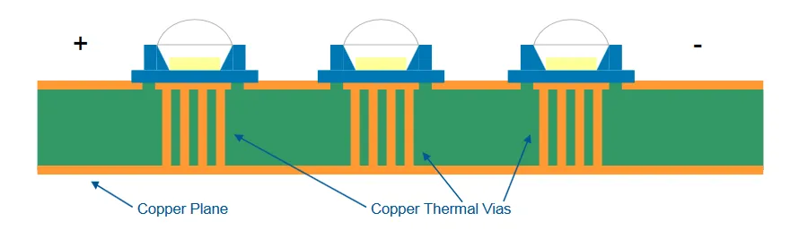
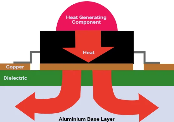
Heat transfer in PCBs occurs through conduction, convection, and radiation, with conduction dominating within the board structure. Copper planes and thermal vias provide low-resistance paths for heat to spread laterally and vertically. Dielectric materials like FR-4 exhibit lower thermal conductivity, around 0.3 W/mK, bottlenecking dissipation in multilayer stacks. Engineers model these as thermal resistance networks, where total resistance sums in series and parallels based on geometry. Radiation contributes minimally at typical operating temperatures below 150°C, while convection depends on airflow and heatsink integration.
Thermal vias PCB elements bridge layers, enhancing via-in-pad or filled via configurations for superior conduction. Plane layers act as heat spreaders, distributing localized hotspots across larger areas. In multilayer PCB heat scenarios, via fields near high-power ICs reduce peak temperatures by channeling heat to outer layers. Analytical models use Fourier's law, q = -k ?T, to estimate fluxes, with k as material conductivity. These principles guide initial sizing before advanced simulations. Accurate modeling prevents underestimation of thermal coupling between adjacent components.
Core Thermal Analysis Techniques for PCB Designers
Analytical Methods for Quick Assessments
Analytical techniques offer rapid insights into steady-state thermal behavior without computational overhead. Engineers apply superposition principles to calculate temperature rises from multiple heat sources using trace width formulas from standards like IPC-2152. For multilayer PCB heat, plane temperature models assume uniform spreading resistance, adjusted for board thickness and copper coverage. These methods suit early-stage PCB design thermal analysis, providing baselines for trace routing and via placement. Limitations arise in transient or nonlinear scenarios, necessitating hybrid approaches. Electric engineers value their simplicity for iterative design loops.
Numerical Simulation Approaches
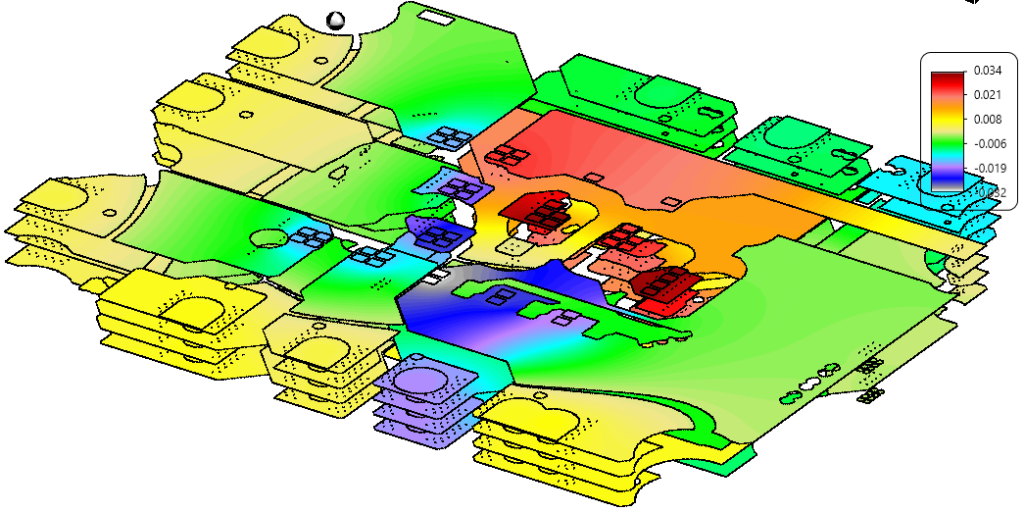
Finite element analysis (FEA) and computational fluid dynamics (CFD) dominate advanced thermal analysis PCB workflows. FEA discretizes the PCB into meshes, solving coupled thermal-electrical equations for transient responses. Tools simulate multilayer stacks, capturing via thermal resistances and board-level convection. CFD extends this by modeling airflow over finned heatsinks or forced convection in enclosures. Validation against experimental data refines boundary conditions like ambient temperature and emissivity. These simulations optimize heat dissipation PCB layouts, minimizing hotspots below component maximum ratings.
In practice, engineers define material properties per JEDEC guidelines for high-density interconnects. Simulations reveal interactions like ground plane shielding effects on trace heating. Parametric studies vary via pitch and diameter to balance electrical and thermal performance. Outputs include isotherm contours and junction-to-ambient resistances, theta JA. For complex multilayer PCB heat profiles, multiphysics coupling includes mechanical stress from thermal expansion.
Experimental Validation Techniques
Infrared thermography captures real-time surface temperatures with high spatial resolution, ideal for populating prototypes. Contact methods like thermocouples measure point-specific data, calibrated against blackbody references for accuracy. Liquid crystal thermography visualizes isotherms on bare boards, sensitive to small gradients. Dye-stain methods reveal flow paths in transient tests, useful for via efficiency. These complement simulations, quantifying errors from model assumptions. PCB design thermal analysis cycles iterate between prediction and measurement for design closure.
Thermal resistance testing per J-STD standards verifies heat dissipation PCB efficacy post-fabrication. Engineers expose boards to controlled power inputs, logging steady-state profiles. Warpage assessments during thermal shock correlate with multilayer PCB heat impacts on flatness. Combining modalities builds confidence in production designs.
Best Practices for Implementing Thermal Analysis in Design
Strategic layer stackup positions power planes adjacent to components for direct heat extraction. Symmetrical builds minimize warpage from asymmetric heating. Thermal vias PCB arrays, with 0.2-0.3 mm diameters on 0.5-1 mm pitch, enhance vertical conduction without excessive capacitance. Filling vias with conductive epoxy boosts performance in high-reliability applications. Engineers aspect-ratio limit vias to under 10:1 for plating uniformity.
Copper pour and balanced trace routing promote uniform spreading. Thicker copper, 2-3 oz/ft2, on inner layers reduces plane resistance. Heat dissipation PCB improves with cutouts or slotted ground planes directing flow. Silkscreen and solder mask emissivity affect radiation, tuned via surface finishes. Simulations guide trade-offs between thermal relief and via density near signals.
Component placement clusters low-power signals away from hotspots. Decoupling capacitors near ICs manage transient thermal spikes. Board-level strategies include edge connectors for heatsink mounting and conformal coatings for environmental robustness. Post-analysis, design reviews flag theta JC exceedances. These practices ensure multilayer PCB heat stays within operational envelopes.
Troubleshooting Common Thermal Issues in Multilayer Designs
Hotspots often trace to undersized traces or isolated vias, confirmed by IR mapping. Delamination signals poor via fill or CTE mismatch, addressed by material selection per IPC guidelines. Simulations predict via voiding risks during reflow. Troubleshooting workflows start with a power budget audit, followed by targeted venting. Case examples show 20-30% temperature drops from optimized via fields, though exact gains vary by stackup. Engineers log discrepancies to refine future models.
Transient analysis catches pulsed power overshoots missed in DC simulations. Oscilloscope-correlated thermal data reveals dynamic behaviors. Fabrication variances like plating thickness impact conduction, necessitating statistical margins. Collaborative reviews between design and thermal teams accelerate resolutions.
Conclusion
Thermal analysis PCB techniques empower electric engineers to conquer multilayer PCB heat challenges through integrated analytical, simulation, and experimental methods. From fundamental conduction paths to advanced FEA models, these tools ensure optimal heat dissipation PCB performance. Best practices like thermal vias PCB optimization and strategic stackups deliver reliable designs compliant with industry benchmarks. Proactive PCB design thermal analysis minimizes risks, extends product life, and supports innovation in dense electronics. Mastering these approaches positions teams for success in high-stakes applications.
FAQs
Q1: What is the role of thermal vias in PCB design thermal analysis?
A1: Thermal vias provide vertical conduction paths in multilayer boards, reducing peak temperatures by channeling heat from inner layers to surfaces. In PCB design thermal analysis, simulations quantify their effectiveness based on count, size, and fill material. Engineers optimize arrays to balance thermal resistance with parasitics, often achieving significant hotspot mitigation. Standards guide via reliability under thermal stress.
Q2: How does multilayer PCB heat affect overall board reliability?
A2: Multilayer PCB heat induces thermal stresses that accelerate fatigue in solder joints and dielectrics. Elevated temperatures promote electromigration in traces, shortening lifespan. Thermal analysis PCB identifies gradients early, enabling mitigations like plane enhancements. Proper management per IPC standards ensures long-term stability.
Q3: Why is FEA important for heat dissipation PCB strategies?
A3: FEA models complex geometries and boundary conditions for accurate temperature predictions in heat dissipation PCB designs. It handles transient effects and multiphysics interactions overlooked by analytical methods. Electric engineers use it to iterate stackups virtually, cutting prototype costs. Validation refines models for production confidence.
Q4: What experimental methods validate thermal analysis PCB results?
A4: IR thermography and thermocouples measure surface and point temperatures on prototypes, benchmarking simulations. Dye-stain tests visualize heat paths through vias. These confirm multilayer PCB heat models, highlighting discrepancies from fabrication tolerances. Iterative testing ensures design robustness.
References
IPC-2221B — Generic Standard on Printed Board Design. IPC, 2012
IPC-2152 — Standard for Determining Current Carrying Capacity in Printed Board Design. IPC, 2009
JEDEC J-STD-020E — Moisture/Reflow Sensitivity Classification for Nonhermetic Surface Mount Devices. JEDEC, 2014


