 ALLPCB


Introduction
Heavy copper PCB materials play a critical role in applications demanding high current handling and robust thermal performance. These materials support copper thicknesses exceeding standard levels, enabling printed circuit boards to manage substantial power loads without excessive heating or failure. Electrical engineers often select heavy copper PCB materials for power supplies, automotive electronics, and industrial controls where reliability under stress is paramount. Understanding the composition and properties of these materials ensures optimal design and manufacturing outcomes. This guide explores heavy copper PCB FR4, high TG variants, and substrate options, providing factory-driven insights aligned with industry standards.
What Are Heavy Copper PCB Materials?
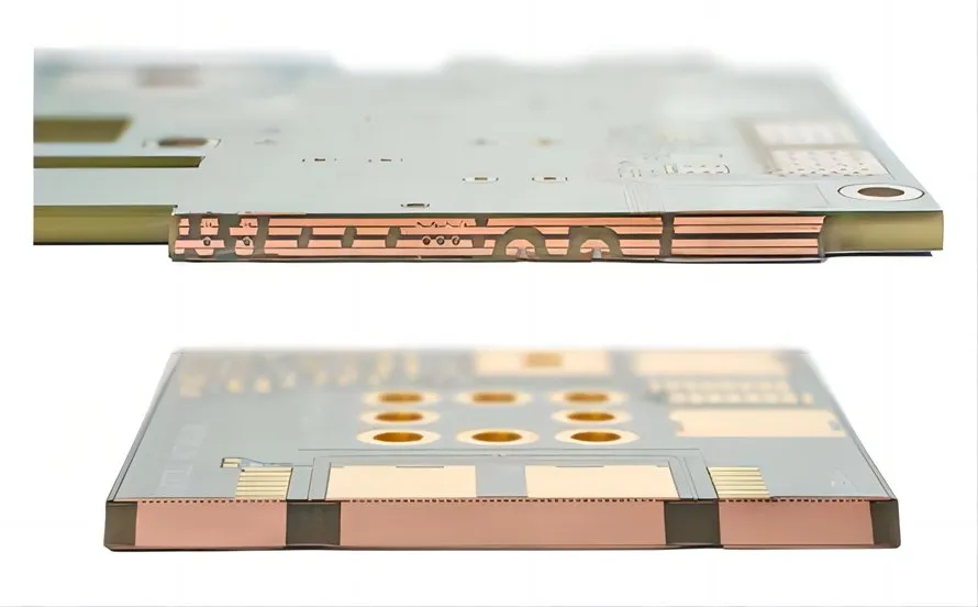
Heavy copper PCB materials refer to substrates and copper foils designed for boards with copper layers thicker than conventional 1 or 2 oz per square foot. Typically, heavy copper denotes thicknesses starting from 3 oz per square foot on both inner and outer layers, supporting higher current densities. The substrate forms the core, providing mechanical support and insulation, while the copper delivers conductivity. Common heavy copper PCB substrates include epoxy-based laminates that maintain integrity during fabrication processes like plating and etching. These materials must withstand the stresses of differential expansion and plating buildup unique to thicker copper.
Factory experience shows that heavy copper PCB materials require careful selection to avoid issues like delamination or uneven etching. Engineers classify them based on copper weight, substrate type, and thermal characteristics. This classification guides applications from moderate power to extreme environments.
Why Heavy Copper PCB Materials Matter
Heavy copper PCB materials excel in high-power scenarios where standard boards falter due to current limitations and thermal buildup. Thicker copper reduces resistance, allowing traces to carry more amperage with minimal voltage drop and heat generation. In power converters and motor drives, these materials prevent hotspots that could degrade components or cause failures. Their relevance grows with electrification trends in vehicles and renewable energy systems, demanding compact yet durable boards.
Beyond conductivity, heavy copper PCB substrates offer enhanced mechanical strength, crucial for multilayer stacks under thermal cycling. Poor material choice leads to warpage or via failures, compromising reliability. Standards like IPC-2221 provide guidelines for current capacity, ensuring designs align with real-world performance. Selecting appropriate heavy copper PCB materials balances cost, manufacturability, and longevity.
Key Types of Heavy Copper PCB Materials
Heavy Copper PCB FR4
Heavy copper PCB FR4 uses the standard flame-retardant epoxy resin reinforced with woven glass fiber as the substrate. This material suits many applications due to its balanced electrical insulation, mechanical stability, and cost-effectiveness. FR4 supports heavy copper plating through its compatibility with electroplating processes, though it demands precise control to manage etching differentials. In fabrication, the substrate's properties influence copper adhesion and overall board flatness.
Engineers favor heavy copper PCB FR4 for prototypes and mid-range power boards, as it processes similarly to standard FR4 but requires adjusted parameters for thicker foils. Its widespread availability streamlines procurement for volume production.
Heavy Copper PCB High TG
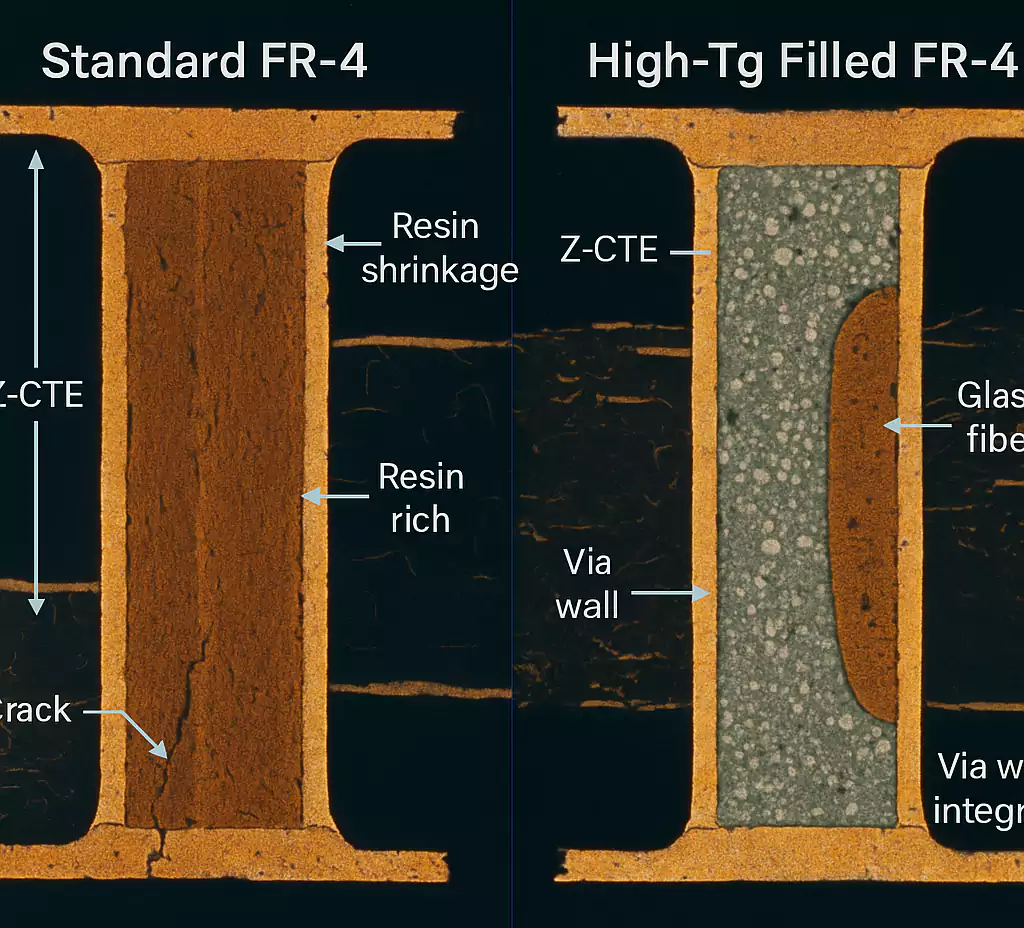
Heavy copper PCB high TG materials feature substrates with elevated glass transition temperature, improving resistance to heat during soldering and operation. These variants maintain structural integrity at higher temperatures compared to standard FR4, reducing risks of softening or delamination in reflow processes. The high TG formulation involves modified resins that enhance thermal stability without sacrificing other properties.
In heavy copper applications, high TG substrates mitigate warpage from asymmetric copper distribution across layers. Factories recommend them for lead-free assembly or environments exceeding typical operating temperatures. IPC-4101 specifications outline requirements for these base materials, ensuring consistency.
Heavy Copper PCB Substrates: Advanced Options
Heavy copper PCB substrates extend beyond FR4 to include high-performance laminates for specialized needs. These may incorporate ceramics or polyimides for superior thermal conductivity or flexibility, though epoxy glass remains dominant. Substrate selection hinges on coefficient of thermal expansion matching with copper to prevent stress cracks.
Advanced heavy copper PCB substrates prioritize low moisture absorption to avoid reliability issues in humid conditions. They support multilayer constructions where interlayer alignment is critical.
Technical Properties of Heavy Copper PCB Materials
The effectiveness of heavy copper PCB materials stems from their interplay of electrical, thermal, and mechanical properties. Copper thickness directly impacts trace resistance and current-carrying capacity, as outlined in design standards. Substrates contribute dielectric strength and dimensional stability, essential for high-layer-count boards.
Thermal management relies on the substrate's ability to dissipate heat from thick copper areas. High current generates localized heating, so materials with favorable heat transfer prevent hotspots. Mechanical properties like rigidity counter the weight and stress of heavy copper, maintaining planarity post-fabrication.
Fabrication reveals that heavy copper PCB materials must endure aggressive etching, where thinner areas etch faster than thick ones. This differential etching demands precise control to achieve uniform traces.
Manufacturing Considerations for Heavy Copper PCBs
Producing boards with heavy copper PCB materials involves adapted processes starting from core preparation. Thicker starting foils or extended electroplating builds copper weight, often requiring multiple plating cycles for uniformity. Lamination under high pressure bonds cores and prepregs, compensating for copper's lower CTE compared to the substrate.
Drilling and plating present challenges, as heavy copper demands larger aspect ratios and robust barrel plating. Factories use pulse plating for void-free fills in vias. Solder mask application must accommodate topography from thick traces.
Post-etch inspection verifies trace integrity per IPC-6012 performance specs. These steps ensure heavy copper PCB materials yield reliable products.
Best Practices for Design and Material Selection
Designers should calculate trace widths using IPC-2221 guidelines, factoring in temperature rise and board stacking. Pair heavy copper with high TG substrates for thermal cycling reliability. Simulate thermal profiles to predict hotspots and adjust copper distribution.
Specify material grades per IPC-4101 to guarantee properties. Balance layer copper weights to minimize warpage; symmetric builds perform best. Incorporate thermal vias under high-current areas for heat spreading.
Procurement teams verify supplier capabilities for heavy copper thicknesses. Prototype testing validates designs before scaling.
Common Challenges and Solutions in Heavy Copper PCB Fabrication
Warpage tops challenges with heavy copper PCB materials, arising from CTE mismatch during cooling. Solutions include constrained lamination and balanced copper layouts. Plating uniformity issues in deep vias resolve with reverse pulse techniques.
Etch factor control prevents undercuts in thick copper; tenting and spray etching help. Solder mask adhesion improves with plasma treatment on uneven surfaces.
Routine testing per IPC standards catches defects early. These factory insights enhance yield.
Conclusion
Heavy copper PCB materials like FR4, high TG, and specialized substrates enable robust high-power electronics. Selecting based on application needs ensures performance and reliability. Adhering to standards optimizes design and manufacturing. Engineers gain confidence through understanding these materials' properties and processes, driving successful implementations.
FAQs
Q1: What are heavy copper PCB materials?
A1: Heavy copper PCB materials consist of thick copper foils, typically 3 oz per square foot or more, paired with substrates like FR4 or high TG laminates. These support high current without excessive heat. Factory processes adapt plating and etching for uniformity. Proper selection per IPC guidelines prevents common failures like warpage.
Q2: How does heavy copper PCB FR4 differ from standard FR4?
A2: Heavy copper PCB FR4 uses the same epoxy glass substrate but handles thicker copper layers through enhanced fabrication. It maintains cost advantages while boosting current capacity. Challenges include differential etching, addressed by precise controls. Ideal for power applications needing reliability.
Q3: When should you choose heavy copper PCB high TG substrates?
A3: Opt for heavy copper PCB high TG when operating temperatures approach or exceed standard FR4 limits, such as in lead-free soldering. The higher glass transition temperature reduces delamination risks. It pairs well with thick copper for thermal stability. Standards like IPC-4101 ensure material consistency.
Q4: What factors influence heavy copper PCB substrate selection?
A4: Key factors include thermal expansion matching, moisture resistance, and mechanical strength for multilayer boards. Heavy copper PCB substrates must support plating stresses. Evaluate per application power and environment. Balanced properties yield flat, durable boards.
References
IPC-4101E — Specification for Base Materials for Rigid and Multilayer Printed Boards. IPC, 2016
IPC-2221B — Generic Standard on Printed Board Design. IPC, 2012
IPC-6012E — Qualification and Performance Specification for Rigid Printed Boards. IPC, 2015
IPC-2152B — Standard for Determining Current Carrying Capacity in Printed Board Design. IPC, 2019


