 ALLPCB


Introduction
In flexible PCB design and rigid-flex PCB applications, copper thickness plays a pivotal role in determining both electrical performance and mechanical reliability. Measured in mils, which provides precise control over conductor dimensions, copper thickness directly influences current-carrying capacity, signal integrity, and the ability to withstand repeated bending. Engineers must carefully select this parameter to balance conductivity needs with the demands of dynamic flexing, where excessive thickness can lead to fatigue failure. Rigid-flex PCB constructions add complexity, as copper varies between rigid and flexible sections to optimize overall functionality. This article explores the engineering principles behind copper thickness choices, focusing on bending stress PCB mitigation and best practices aligned with industry standards.
Defining Copper Thickness in Mils for Flex Circuits
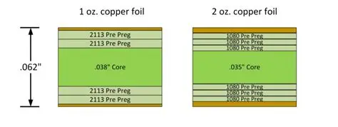
Copper thickness in printed circuit boards is typically specified in ounces per square foot, but mils offer a direct measure of foil height, essential for flexible PCB design calculations. One ounce copper equates to approximately 1.4 mils of thickness when spread evenly over one square foot, while half-ounce is about 0.7 mils and two-ounce reaches 2.8 mils. These values represent the starting point before etching and plating, which can alter final dimensions. In flex circuits, thinner foils reduce overall stack-up height, enabling tighter bend radii without compromising trace integrity. Thicker copper suits high-current paths but demands wider traces to manage heat dissipation effectively.
Engineers convert ounce weights to mils for stress analysis during dynamic flexing, as strain distributions depend on exact dimensions. Standard fabrication processes maintain tight tolerances on these thicknesses to ensure consistency across production runs. Polyimide-based flex materials pair well with these foils, supporting adhesion and flexibility.
Mechanical Implications: Bending Stress PCB and Copper Thickness
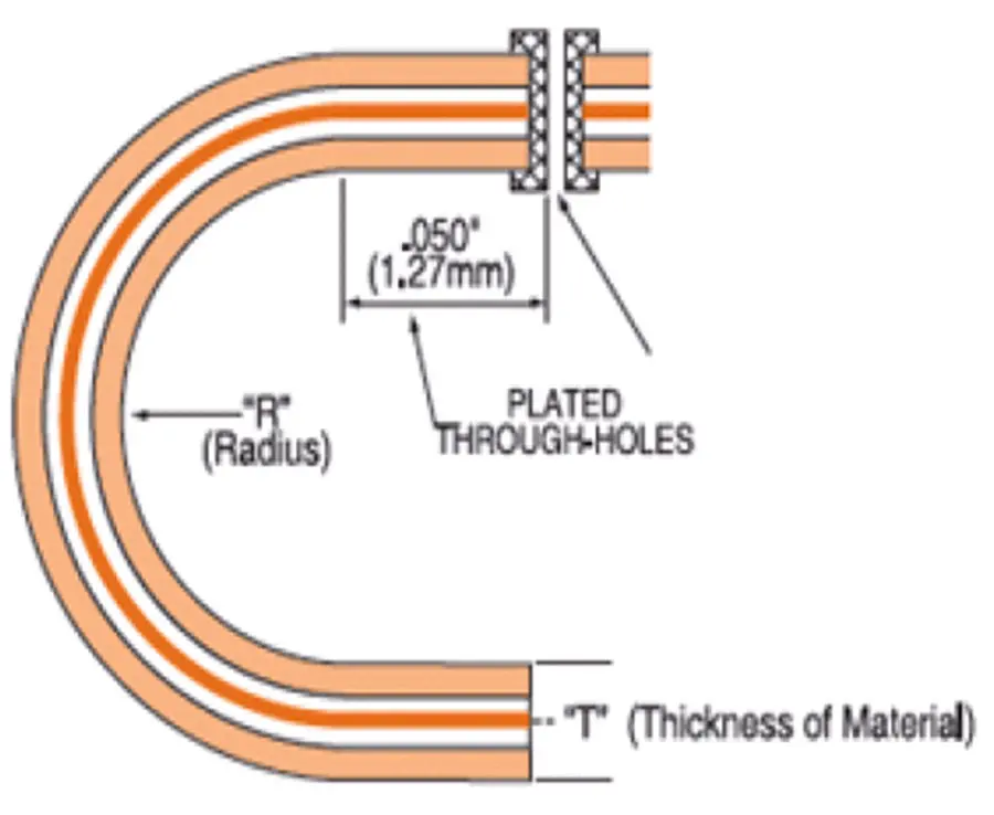
Bending stress PCB arises primarily from differential strain across the circuit layers during flexure, with copper thickness amplifying this effect. In a bent flex section, the outermost copper foil experiences tensile stress proportional to its distance from the neutral axis and inversely to the bend radius. Thicker copper, such as 2 mils or more, shifts the neutral axis and increases peak strain, potentially leading to microcracks under repeated cycles. For dynamic flexing applications like wearable devices or hinges, this stress accelerates fatigue, reducing lifespan. IPC-2223 provides guidelines for calculating minimum bend radii based on copper thickness and layer count, recommending ratios like 10 times the total flex thickness for static bends.
The strain equation, ε = (t / 2) / R—where t is copper thickness in mils and R is bend radius—highlights why thinner foils excel in high-flex environments. Compression on the inner side can cause delamination if copper ductility is insufficient. Rolled annealed copper, preferred for flex over electrodeposited types, offers better grain structure for enduring bending stress PCB without fracturing. Material modulus and coverlay thickness further modulate these stresses, requiring holistic stack-up optimization.
 )
)
Copper Thickness for Flex: Static vs. Dynamic Applications
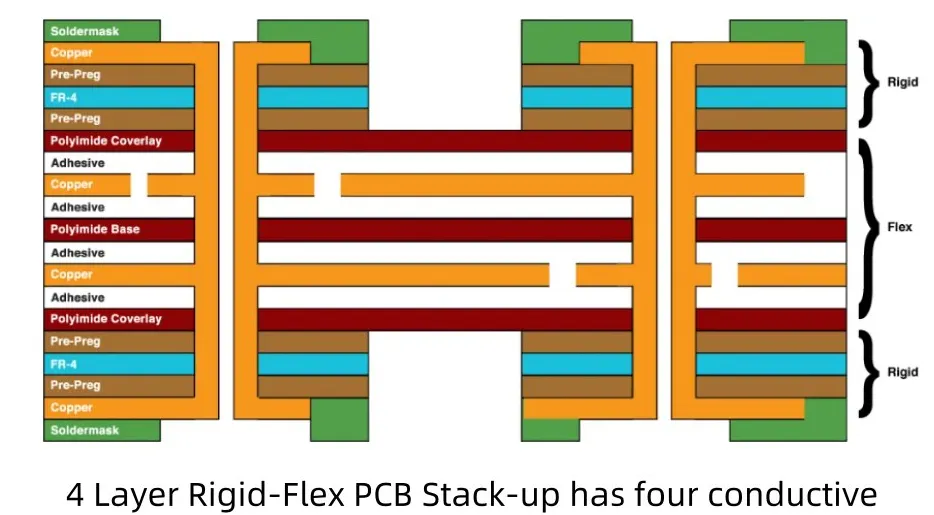
In static flexible PCB design, where bends occur infrequently, copper thicknesses up to 2 mils support robust electrical performance without excessive risk. Dynamic flexing, however, necessitates half-ounce or one-ounce foils to keep strain below 0.3% for millions of cycles. Rigid-flex PCB designs often employ graduated thicknesses: thinner in pure flex zones and heavier in rigid areas for component mounting stability. Transition zones demand careful plating to avoid stress risers at material interfaces. Coverlay openings and trace routing must align with copper specs to prevent cracking propagation.
Adhesive choice influences how copper conforms during flex, with no-flow adhesives minimizing voids under thicker foils. For multilayer rigid-flex PCB, outer layers in flex regions stay thin to preserve bend radius compliance. IPC-6013 outlines qualification tests, including flex endurance cycling, to verify copper integrity post-fabrication. These standards ensure designs meet performance thresholds under simulated use conditions.
Best Practices in Rigid-Flex PCB Copper Specification
Select copper thickness for flex based on application demands, starting with thermal and electrical simulations to validate choices. Position high-current traces on inner flex layers to shield them from maximum bending stress PCB exposure. Use 0.7 to 1.4 mil foils for dynamic regions, widening traces proportionally for ampacity. In rigid-flex PCB stack-ups, frame rigid sections with heavier copper while tapering flex tails. Verify plating uniformity, as uneven buildup exacerbates fatigue in dynamic flexing scenarios.
Incorporate tear stops and strain-relief features around bends, scaled to copper dimensions. Simulate bend cycles using finite element analysis to predict failure points tied to mil thicknesses. Collaborate with fabricators early to align on achievable weights and tolerances. These steps enhance reliability while adhering to IPC guidelines for flexible PCB design.
Optimizing for Long-Term Dynamic Flexing Reliability
Dynamic flexing imposes cyclic loading, where copper thickness dictates fatigue life through crack initiation thresholds. Thinner foils distribute strain more evenly, extending cycles before propagation. Electrodeposited copper suits rigid areas but risks brittleness in flex; rolled types dominate high-cycle needs. Solder mask or coverlay encapsulation protects edges, crucial for thicker foils prone to nicks.
Test protocols per IPC-6013 involve repeated flexing over mandrels sized to design radii, inspecting for opens or resistance shifts. Adjust copper based on results, iterating for marginal cases. Multilayer flex requires symmetric builds to center the neutral axis, minimizing copper-specific stresses.
Troubleshooting Common Issues in Copper-Heavy Flex Designs
Excessive bending stress PCB manifests as trace fractures or delamination, often traced to over-thick copper in tight radii. Diagnose via cross-section microscopy, measuring final mil thicknesses against specs. Remedy by down-gauging to 0.7 mils and increasing radii per IPC-2223 ratios. Impedance mismatches from thick foils demand length matching in high-speed rigid-flex PCB signals.
Environmental factors like humidity swell dielectrics, amplifying copper strain; bake-out pre-flex mitigates this. For dynamic flexing failures, audit foil type and anneal state. Proactive DFMA reviews catch thickness mismatches early.
Conclusion
Copper thickness in mils remains a cornerstone of successful flexible PCB design and rigid-flex PCB implementation, directly governing bending stress PCB and dynamic flexing endurance. Thinner foils enable compact, reliable bends while thicker ones bolster power handling in rigid zones. Adhering to standards like IPC-2223 and IPC-6013 ensures designs withstand real-world rigors. Engineers achieve optimal outcomes by integrating simulations, material science, and iterative testing. Prioritizing these factors yields durable circuits that meet performance goals without compromise.
FAQs
Q1: What is the ideal copper thickness for flex in dynamic flexing applications?
A1: For dynamic flexing, select 0.5 to 1 oz copper, equating to 0.7 to 1.4 mils, to minimize bending stress PCB. This range supports tight radii and millions of cycles per IPC-2223 guidelines. Thicker foils suit static bends but risk fatigue in motion-heavy flexible PCB design. Always simulate strain distributions for validation.
Q2: How does copper thickness affect bend radius in rigid-flex PCB?
A2: Thicker copper increases required bend radius to limit strain, often 10 to 100 times total flex thickness depending on layers and cycles. In rigid-flex PCB, flex sections use thinner mils for compliance, transitioning smoothly to rigid power planes. IPC-6013 testing confirms radius adequacy under load.
Q3: Why prioritize thinner copper thickness for flex in high-cycle uses?
A3: Thinner copper reduces peak tensile stress during dynamic flexing, preserving ductility and preventing microcracks. It lowers overall stack-up height for compact flexible PCB design. Standards recommend this for applications like sensors or cables undergoing frequent motion.
Q4: Can copper thickness vary within a single rigid-flex PCB design?
A4: Yes, rigid-flex PCB commonly features varying thicknesses: thin in flex tails for bending stress PCB relief, heavier in rigid cores for components. This gradient optimizes electrical and mechanical traits. Design per IPC-2223 to avoid transition failures.
References
IPC-2223E — Sectional Design Standard for Flexible/Rigid-Flexible Printed Boards. IPC, 2020
IPC-6013D — Qualification and Performance Specification for Flexible Printed Boards. IPC, 2017
IPC-6012E — Qualification and Performance Specification for Rigid Printed Boards. IPC, 2017


