 ALLPCB


Introduction
In the realm of high-power electronics, 2oz copper PCBs stand out for their ability to handle elevated current loads while maintaining structural integrity. These boards feature copper foil that is twice as heavy as standard 1oz configurations, enabling superior thermal performance and reduced resistive losses in demanding applications. Proper 2oz copper PCB layout becomes critical as thicker copper alters traditional design dynamics, influencing everything from trace routing to heat dissipation. Electrical engineers must master specific PCB design rules to prevent issues like overheating or voltage drops that could compromise circuit reliability. This article delves into essential layout guidelines, including strategies for PCB trace width calculation and PCB via design, ensuring robust performance in power-heavy designs. By following structured approaches, designers can optimize board efficiency without unnecessary complexity.
What Is a 2oz Copper PCB and Why It Matters
A 2oz copper PCB refers to a printed circuit board where the copper conductors weigh 2 ounces per square foot, providing greater cross-sectional area compared to lighter weights like 1oz. This increased copper mass translates to lower resistance per unit length, making it ideal for applications requiring high current densities, such as power converters, motor drives, and LED lighting arrays. In industries like automotive electronics and renewable energy systems, 2oz copper PCB layouts support higher power throughput while minimizing the physical footprint of traces and planes. The relevance intensifies in modern designs where compact form factors demand efficient heat management without relying solely on external cooling. Engineers benefit from reduced voltage drops across traces, which preserves signal integrity in mixed analog-digital environments. Ultimately, adopting 2oz copper elevates design margins, aligning with the push for reliable, high-performance hardware.
Beyond basic conductivity, the thicker copper enhances mechanical robustness during thermal cycling, reducing the risk of cracking in solder joints or delamination under stress. For electrical engineers tackling dense layouts, this material choice simplifies routing by allowing narrower traces for equivalent current ratings versus thinner foils. However, it introduces unique challenges in etching precision and impedance control, necessitating tailored PCB design rules. Ignoring these can lead to manufacturing defects or field failures, underscoring the need for precise layout strategies from the outset.
Core Technical Principles Governing 2oz Copper PCB Layout
The foundation of effective 2oz copper PCB design rests on understanding current-carrying capacity, which scales with copper thickness due to larger cross-sectional area. Thicker foils exhibit lower resistance, but current density limits still apply to avoid excessive heating from I2R losses. Standards like IPC-2152 provide the framework for calculating safe operating limits, factoring in ambient temperature, trace length, and board thickness. Electrical engineers must consider how elevated copper weight shifts thermal profiles, as heat spreads more effectively across wider paths but concentrates at bends or junctions. This principle guides 2oz copper PCB layout by prioritizing wide power planes over serpentine traces where possible.
Another key mechanism is thermal expansion mismatch between copper and substrate materials, which becomes pronounced in heavier copper weights during reflow or operation. Differential expansion can induce stress on vias and pads, potentially leading to micro-cracks if not mitigated through balanced stackups. Skin effect also plays a role at higher frequencies, where current crowds the conductor surface, slightly reducing effective thickness benefits for AC signals. Logical layout decisions, such as symmetric plane pours and thermal reliefs, counteract these effects systematically. By integrating these principles, designs achieve uniform temperature distribution, extending component lifespan.
Electromigration poses a long-term reliability concern, accelerated by high current densities in thin sections despite overall thicker copper. Engineers apply derating factors to ensure atomic migration does not degrade traces over time. Impedance characteristics shift too, with 2oz copper lowering characteristic impedance in controlled lines, requiring adjusted spacing for high-speed signals. These interconnected principles demand a holistic approach to PCB design rules, blending electrical, thermal, and mechanical analyses.
Essential PCB Design Rules for 2oz Copper Layouts
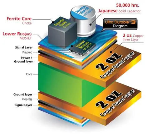
Adhering to established PCB design rules ensures manufacturability and performance in 2oz copper boards. Minimum trace width expands compared to 1oz due to etching undercuts on thicker foils, allowing designers to maintain current capacity with less board real estate. Clearance and spacing rules follow IPC-2221 guidelines, scaled for voltage levels and pollution degrees to prevent arcing or shorts. For power sections, engineers prioritize solid planes over segmented traces to minimize inductance and EMI. Layer sequencing matters, with 2oz copper often placed on inner layers for shielding while outer layers handle signals.
A critical tool in this process is the PCB trace width calculator, which engineers use to determine optimal dimensions based on current, allowable temperature rise, and copper weight. Inputs include ambient conditions and board stackup, outputting widths that keep junction temperatures within safe bounds per industry charts. For 2oz copper, calculators reveal narrower traces suffice for given amps versus lighter weights, optimizing space in dense layouts. Always verify results against full thermal simulations, as external factors like airflow influence real-world behavior. Pairing this with annular ring specs prevents via breakout failures during fabrication.
Routing topology influences overall integrity, favoring orthogonal grids over diagonals to ease CAM processing. Annular rings around pads must accommodate thicker copper's etch factor, typically wider to ensure robust plating. Ground return paths demand low-impedance symmetry, often via extensive stitching to couple planes effectively.
Optimizing PCB Via Design for 2oz Copper Boards
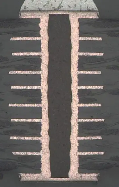
Vias serve as vertical interconnects in multilayer 2oz copper PCBs, but their design requires special attention due to current funneling effects. Through-hole vias handle higher currents than microvias, with plating thickness scaled to match outer copper weight for uniform resistance. In power distribution, arrays of vias distribute load, preventing hotspots at single points. PCB via design rules dictate minimum drill sizes and aspect ratios, limiting depth-to-diameter to avoid plating voids per IPC standards.
Filled vias enhance thermal conductivity in high-heat zones, encapsulating conductive epoxy to bridge layers seamlessly. For 2oz copper, blind or buried vias conserve board thickness while supporting heavy current paths. Engineers calculate via thermal resistance alongside trace widths, ensuring the chain's weakest link does not bottleneck performance. Stitching vias along plane edges maintain return current flow, reducing loop inductance in fast-switching circuits.
Common pitfalls include insufficient land sizes, leading to pad lift-off under thermal stress from mismatched CTE. Logical placement clusters vias near high-current components, with tenting on unused holes to block solder wicking.
Best Practices and Troubleshooting for 2oz Copper Layouts
Implement best practices by starting with stackup planning, allocating 2oz layers strategically for power and ground to sandwich signals. Use pour-over techniques for power distribution, fracturing planes only at splits with fanouts. During DRC checks, enforce rules for neck-downs at transitions, widening traces preemptively. Simulate parasitics early, as thicker copper alters capacitance between layers.
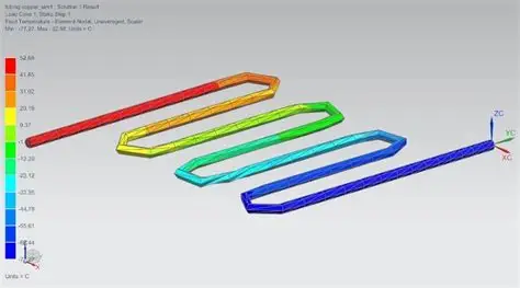
Troubleshooting hotspots involves infrared imaging post-prototype, correlating to trace calculations. If overheating persists, redistribute vias or add copper balancing. For EMI issues, ensure plane overlaps exceed trace lengths by design rules. These steps yield reliable 2oz copper PCB layouts.
Conclusion
Mastering 2oz copper PCB design hinges on integrating PCB design rules, precise PCB trace width calculations, and thoughtful PCB via design. Thicker copper unlocks high-power potential but demands disciplined layout to manage thermal and electrical challenges. By referencing standards like IPC-2152 and IPC-2221, engineers achieve balanced, efficient boards. Key takeaways include prioritizing planes, verifying calculator outputs, and optimizing vias for current sharing. Applying these guidelines elevates design quality, ensuring longevity in demanding applications.
FAQs
Q1: What are the key PCB design rules for 2oz copper PCB layout?
A1: PCB design rules for 2oz copper PCB layout emphasize wider clearances, adjusted trace widths, and robust annular rings to account for etching characteristics of thicker foil. Follow IPC-2221 for spacing based on voltage and environment, while ensuring plane splits include adequate fanouts. Stackup symmetry prevents warpage, and DRC verifies manufacturability. These rules support high-current paths without compromising isolation.
Q2: How does a PCB trace width calculator work for 2oz copper?
A2: A PCB trace width calculator for 2oz copper inputs current, temperature rise, ambient conditions, and layer position to output dimensions per IPC-2152 charts. Thicker copper allows narrower traces for the same ampacity, optimizing space. Engineers cross-check with simulations for airflow effects. This tool streamlines layout while upholding thermal limits.
Q3: Why is PCB via design critical in 2oz copper PCBs?
A3: PCB via design in 2oz copper PCBs prevents current bottlenecks and thermal hotspots by using arrays or filled types for even distribution. Plating matches copper weight to avoid resistance steps, with aspect ratios controlled per standards. Proper lands and stitching maintain integrity under stress. Neglect leads to failures in power delivery.
Q4: What common issues arise in 2oz copper PCB layout and how to avoid them?
A4: Common issues in 2oz copper PCB layout include uneven etching and via stress from CTE mismatch. Avoid by selecting appropriate min widths, symmetric stackups, and thermal reliefs. Prototype testing with thermal scans identifies problems early. Adhering to design rules ensures reliable performance.
References
IPC-2152B — Standard for Determining Current Carrying Capacity in Printed Electronic Equipment. IPC, 2009
IPC-2221B — Generic Standard on Printed Board Design. IPC, 2003
IPC-6012E — Qualification and Performance Specification for Rigid Printed Boards. IPC, 2015


