 ALLPCB


Introduction
High-speed digital PCB design faces mounting challenges as data rates climb into the multi-gigabit per second range. Signal integrity issues such as attenuation, reflections, and crosstalk can degrade performance, leading to bit errors and system failures. Engineers often overlook copper thickness as a key lever for mitigation, yet opting for 2oz copper in these designs offers tangible benefits for 2oz copper PCB signal integrity. This thicker copper reduces resistive losses and supports better impedance control, crucial for maintaining clean signals over long traces. By understanding how 2oz copper integrates into high speed PCB design workflows, designers can achieve superior signal loss reduction PCB outcomes without compromising manufacturability. This article explores the principles, practical strategies, and best practices for leveraging 2oz copper effectively.
Understanding Copper Thickness and Its Role in PCBs
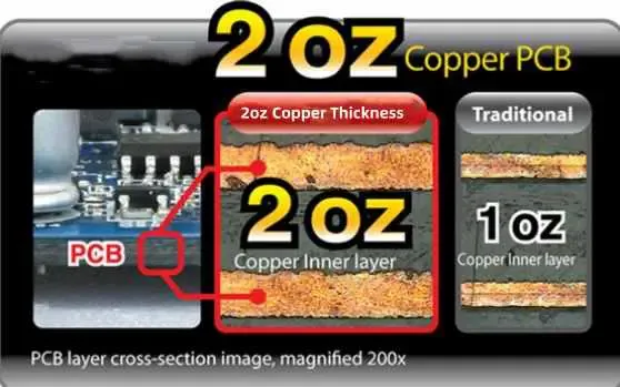
Copper thickness in PCBs is measured in ounces per square foot, where 1oz corresponds to approximately 35 micrometers and 2oz to 70 micrometers after plating. Standard designs default to 1oz for signal layers due to finer feature sizes, but high-speed applications demand reevaluation. Thicker 2oz copper provides lower DC resistance, which translates to reduced ohmic losses in traces carrying fast-edged signals. In high speed PCB design, this matters because even small resistive contributions compound over length, exacerbating attenuation. Moreover, 2oz copper enhances power delivery stability, indirectly bolstering overall signal integrity by minimizing voltage droop under load. Engineers must balance this with etching challenges, as thicker foils require wider traces to avoid undercuts.
Why 2oz Copper Enhances Signal Integrity in High-Speed Designs
Signal integrity in high-speed digital PCBs hinges on minimizing attenuation and preserving waveform fidelity. Conductor losses dominate at frequencies where skin effect confines current to the trace surface, but 2oz copper still offers advantages by providing a larger effective conducting volume below the skin depth. For data rates up to 10 Gbps, where fundamental frequencies reach several GHz, the reduced bulk resistance lowers insertion loss compared to 1oz equivalents. This is particularly evident in long traces or buses, where cumulative loss could otherwise close eye openings. Additionally, 2oz copper supports impedance control PCB strategies by allowing precise trace width adjustments to hit target characteristic impedances like 50 or 100 ohms. Field solver simulations consistently show 1-2 dB less attenuation per inch in 2oz designs under matched conditions.
Dielectric losses remain independent of copper thickness, but the overall attenuation budget improves with 2oz, freeing margin for other optimizations. Power planes benefit immensely, as thicker copper reduces plane resistance and inductance, stabilizing reference voltages for coupled signals. Crosstalk is marginally lower due to better return path continuity. However, surface roughness must be controlled, as it amplifies skin effect losses regardless of thickness. IPC-2221 guidelines emphasize copper weight selection based on current capacity and thermal rise, which align with signal integrity needs in multilayer stacks.
Technical Mechanisms: Skin Effect, Attenuation, and Impedance
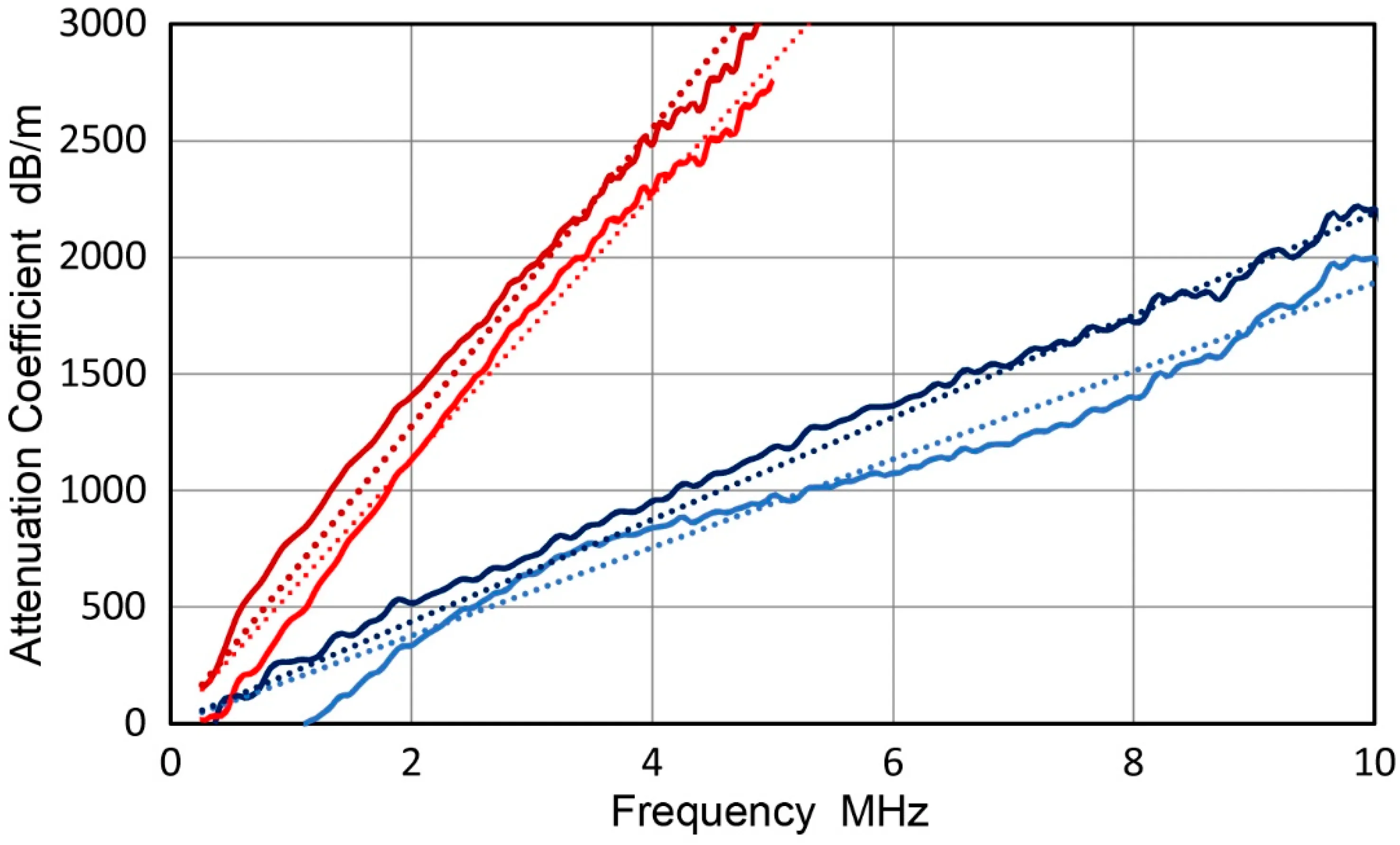
Skin effect causes AC current to flow primarily within a depth δ ≈ 66 / √f micrometers for copper at frequency f in MHz. At 1 GHz, δ is about 2 micrometers, so both 1oz and 2oz exceed this, but thicker copper mitigates non-uniformity from foil profile variations. Resistive loss per unit length scales with surface resistance Rs = √(π f μ / σ), modulated by roughness factor. 2oz copper's smoother post-etch surfaces in controlled processes yield lower effective Rs, enhancing 2oz copper PCB signal integrity. Attenuation α totals conductor and dielectric components: α_c = Rs / (2 Z0 W), where W is trace width, underscoring the need for width scaling in thicker copper.
Impedance control PCB demands recalibration for 2oz. Characteristic impedance Z0 drops with conductor thickness t per Z0 ≈ (87 / √(εr + 1.41)) * ln(5.98 h / (0.8 w + t)), requiring wider w to compensate. For a microstrip 50Ω on 100μm dielectric, 1oz might need 120μm width, while 2oz demands 150-160μm. This wider geometry reduces slotline modes and improves mode confinement. Signal loss reduction PCB via 2oz also stems from lower series inductance in bends and vias, as thicker walls handle plating better. Simulations reveal eye height improvements of several percent in backplane channels.
In stripline configurations, symmetric 2oz planes sandwiching signals yield ultra-low loss PDNs. IPC-6012 performance specs validate minimum copper thicknesses for high-reliability boards, ensuring plating uniformity critical for these effects.
Practical Best Practices for Implementing 2oz Copper
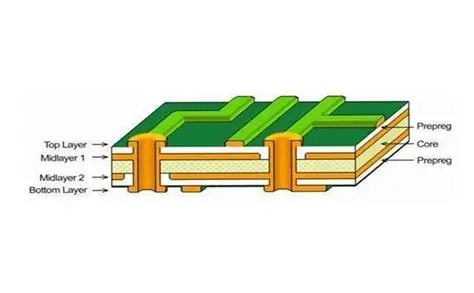
Start with stackup planning: position 2oz on inner layers for signals where etching precision is less demanding than outer fine-lines. Use asymmetric buildup if outer layers need 1oz for HDI features. For impedance control, employ 2D/3D field solvers early to generate width tables versus dielectric height and εr. Target tolerances of ±10% Z0, achievable with 2oz via relaxed aspect ratios during etching.
Routing guidelines include minimizing vias with back-drilling and stitching for returns. Pair 2oz signals with low-Dk dielectrics to isolate conductor benefits. Manufacturing considers panel plating for uniform 2oz buildup, avoiding flash plating pitfalls. Test coupons per IPC standards verify thickness post-etch, typically 50-60μm finished for 2oz start.
Thermal management improves, as 2oz spreads heat from drivers/receivers, reducing jitter from temperature gradients. For signal loss reduction PCB, segment long traces into repeaters only if 2oz savings fall short.
Troubleshooting Common Issues with 2oz Copper Designs
Designers encounter etching asymmetry in 2oz, leading to impedance drift. Mitigate by specifying reverse-treated foil and tenting outer layers. High-frequency simulations may predict excessive width, crowding boards; hybrid 1oz/2oz stacks resolve this. Warpage from CTE mismatch increases with thickness, so balance with core constraints.
Via stub resonances amplify if plating is thin; electroplated 2oz vias extend stub mitigation. Eye diagram closure post-layout signals PDN weakness; thicken plane pairs accordingly.
Conclusion
Leveraging 2oz copper unlocks significant gains in 2oz copper PCB signal integrity for high speed PCB design. By slashing resistive losses and enabling robust impedance control PCB, it delivers measurable signal loss reduction PCB across digital channels. Adhering to structured stackups, precise width calculations, and standard-compliant processes ensures reliable outcomes. Electrical engineers can confidently specify 2oz where simulations justify, balancing performance against density tradeoffs. Future designs at escalating speeds will increasingly rely on such optimizations for margin.
FAQs
Q1: What are the main benefits of 2oz copper for signal integrity in high-speed PCBs?
A1: 2oz copper reduces conductor losses through lower resistance, improving attenuation performance in traces up to several GHz. It supports precise impedance control by allowing wider traces for target Z0 while enhancing PDN stability. This leads to better eye diagrams and fewer bit errors in high speed PCB design applications. Overall, it provides signal loss reduction PCB without exotic materials.
Q2: How does copper thickness affect impedance control in PCBs?
A2: Thicker 2oz copper lowers characteristic impedance for given geometry, necessitating wider traces to maintain 50Ω or 100Ω specs. Field solvers account for this shift accurately in stackups. Proper control ensures minimal reflections, vital for 2oz copper PCB signal integrity. IPC-2221 aids in deriving safe dimensions.
Q3: When should engineers choose 2oz over 1oz copper in high-speed designs?
A3: Opt for 2oz in designs with long traces, high current signals, or tight loss budgets below 10 Gbps. It excels where skin effect losses compound with resistance. Avoid in ultra-dense HDI if width constraints bind. Simulations confirm gains for impedance control PCB needs.
Q4: Can 2oz copper help with signal loss reduction in digital backplanes?
A4: Yes, by minimizing ohmic contributions and improving return paths, 2oz lowers insertion loss per channel length. Combined with low-loss dielectrics, it extends reach. This bolsters overall signal integrity in multi-gigabit links.
References
IPC-2221B — Generic Standard on Printed Board Design. IPC, 2003
IPC-6012E — Qualification and Performance Specification for Rigid Printed Boards. IPC, 2017
IPC-2152 — Standard for Determining Current Carrying Capacity in Printed Board Design. IPC, 2009





