 ALLPCB


Introduction
In modern electronics, printed circuit boards (PCBs) operate at increasingly higher speeds, placing greater demands on signal integrity. Electrical engineers designing high-frequency circuits must carefully consider every aspect of the layout, including trace dimensions. Minimum line width, often the smallest allowable trace dimension in a design, plays a pivotal role in balancing board density with performance reliability. Narrower traces enable more compact layouts, but they introduce challenges related to impedance mismatches and signal degradation. This article explores how PCB signal integrity trace width influences overall system behavior, particularly through the lens of minimum line width signal reflection and impedance control trace width strategies. By understanding these relationships, engineers can optimize designs for robust operation in demanding applications.
Signal integrity issues arise when signals distort during propagation, leading to errors in data transmission or timing violations. Factors such as reflections, attenuation, and crosstalk become pronounced in high-speed environments. Minimum line width decisions directly affect these phenomena because manufacturing tolerances scale with trace dimensions. Engineers pushing for finer lines to achieve higher routing density risk exacerbating signal reflections if not managed properly. Adhering to established guidelines ensures that performance goals align with fabrication capabilities.
Understanding Minimum Line Width in PCB Design
Minimum line width refers to the thinnest conductor trace that a fabrication process can reliably produce while meeting quality criteria. This parameter sets the lower bound for routing in dense boards, influencing both manufacturability and electrical characteristics. In PCB design, engineers specify minimum line widths based on process capabilities, typically starting from standard production limits and adjusting for advanced features. Why does this matter for signal integrity? Narrow traces alter the characteristic impedance of transmission lines, potentially causing mismatches that degrade signal quality.
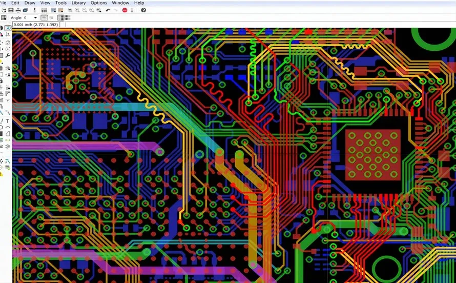
The relevance intensifies in multilayer boards where inner layers carry critical high-speed signals. Fabrication processes like photolithography and etching define achievable resolutions, with tighter controls required for finer widths. Electrical engineers must evaluate trade-offs between density and performance early in the design phase. Industry standards such as IPC-2221 provide foundational guidelines for conductor sizing, emphasizing the need for widths that support intended current levels and spacing rules. Ignoring these can lead to yield issues or field failures.
Beyond density, minimum line width impacts thermal management and reliability under stress. Narrower conductors exhibit higher resistance, leading to greater ohmic losses, especially at elevated frequencies. Engineers often simulate these effects to predict real-world behavior.
The Role of Trace Width in Signal Integrity
Trace width fundamentally determines the characteristic impedance of a PCB transmission line, a key factor in PCB signal integrity trace width considerations. Wider traces lower impedance by increasing the conductor's effective area relative to the reference plane, while narrower ones raise it. This relationship stems from transmission line theory, where impedance Z0 depends on inductance per unit length and capacitance per unit length. For microstrip and stripline configurations common in PCBs, trace width directly modulates these parameters alongside dielectric thickness and material properties.
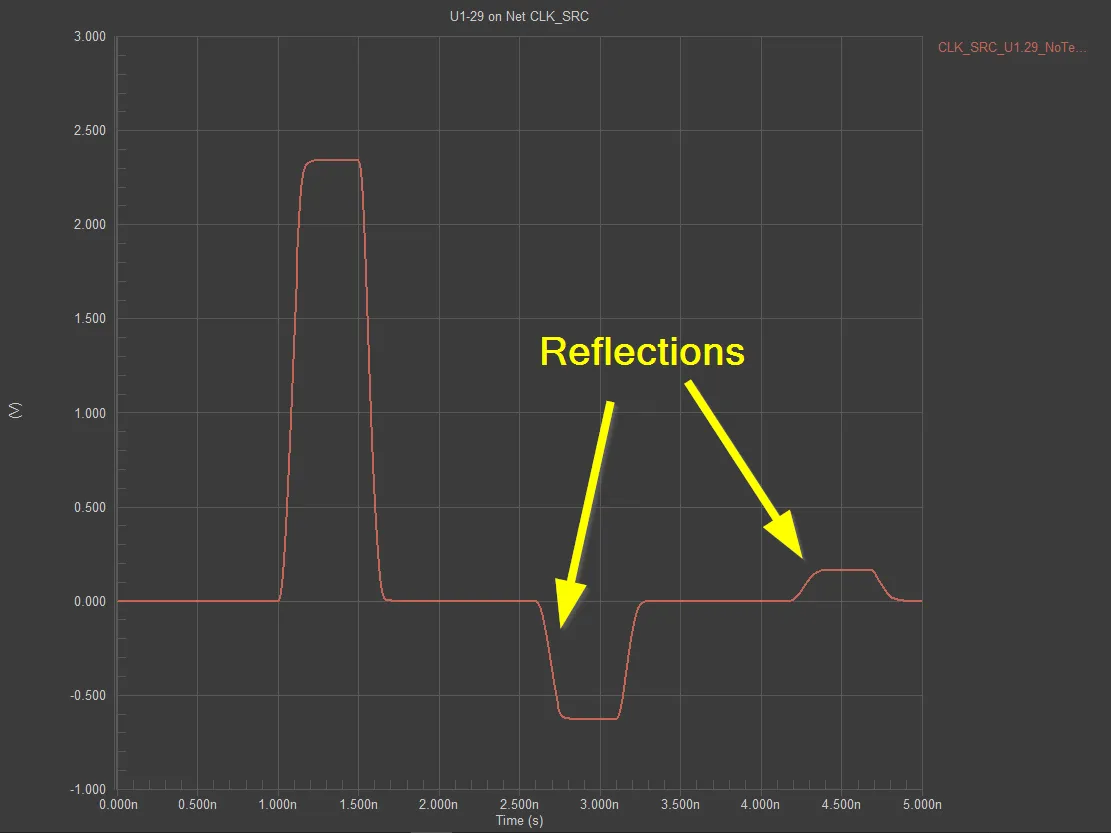
Signal reflections occur at impedance discontinuities, such as transitions between traces of different widths or vias. Minimum line width signal reflection becomes critical when designs incorporate the finest traces, as manufacturing variations amplify mismatches. A slight etch undercut on a narrow trace can shift its impedance significantly, reflecting portions of the incident signal back toward the source. This reflected energy superimposes on subsequent signals, distorting waveforms and reducing eye opening in high-speed links.
Crosstalk also ties to trace width through capacitive and inductive coupling. Adjacent narrow traces with insufficient spacing intensify near-end and far-end crosstalk, compromising noise margins. Engineers mitigate this by applying spacing rules proportional to width, often three times the trace width for sensitive nets.
Mechanisms of Signal Degradation from Narrow Minimum Line Widths
Narrow minimum line widths heighten attenuation due to increased series resistance and skin effect at gigahertz frequencies. Skin effect confines current to the trace surface, effectively reducing cross-sectional area and raising losses proportional to the square root of frequency. Engineers observe this as insertion loss in S-parameter measurements, where finer traces show steeper roll-off. Combined with dielectric losses, this limits signal reach on long traces.
Impedance control trace width optimization counters these effects by tailoring dimensions to target Z0 values, typically 50 ohms single-ended or 100 ohms differential. Sudden width changes, common near components or fanouts, create stubs that reflect signals based on the reflection coefficient formula. The magnitude depends on the impedance step and rise time; fast edges from modern drivers exacerbate ringing.
Dielectric nonuniformity further complicates narrow traces, as fab variations in copper height alter field distribution more dramatically. Propagation delay skew across matched lines can desynchronize differential pairs, leading to common-mode noise conversion.
Standards like IPC-6012 outline performance specifications that indirectly address these through conductor integrity requirements. Compliance ensures traces maintain dimensional stability post-fabrication.
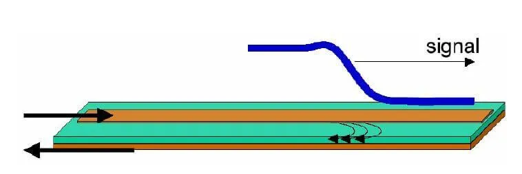
Electromagnetic interference (EMI) worsens with narrow traces due to higher radiation from unbalanced fields. Return currents spread if reference planes have gaps, amplifying emissions.
Best Practices for Impedance Control and Minimum Line Width
Engineers achieve impedance control trace width by using field solvers during layout to predict Z0 from stackup details. Start with a defined stackup, specifying copper weights, dielectric thicknesses, and materials. Iterate trace widths to hit targets, accounting for fab tolerances like ±10% etch control. Length-matching critical nets minimizes skew.
Apply the 3W rule: space parallel traces at least three times the maximum trace width to suppress crosstalk below -30 dB. For minimum line width signal reflection avoidance, taper transitions smoothly rather than abrupt steps. Simulate time-domain reflectometry (TDR) to verify continuity.
Layer assignment matters; route high-speed signals on inner layers with solid references for better confinement. Avoid splitting planes under traces to prevent impedance jumps.
Incorporate test coupons on panels for post-fab TDR verification, correlating measurements to design intent. This practice, aligned with quality standards, catches discrepancies early.
Use via optimization: back-drill or blind vias reduce stubs, complementing trace width efforts.
- Factor: Trace Width — Effect on Impedance: Inverse relationship — Best Practice: Widen for lower Z0
- Factor: Dielectric Height — Effect on Impedance: Inverse — Best Practice: Standardize thicknesses
- Factor: Copper Thickness — Effect on Impedance: Minor decrease — Best Practice: Use 1 oz default
- Factor: Dielectric Constant — Effect on Impedance: Inverse square root — Best Practice: Select low-loss materials
Troubleshooting Common Signal Integrity Issues Related to Trace Width
Engineers often encounter eye closure from reflections traced to inconsistent minimum line widths across revisions. Analyze with vector network analyzer (VNA) sweeps; peaks in return loss indicate mismatches. Correlate to layout by overlaying TDR traces on gerbers.
Attenuation hotspots on narrow traces signal skin effect dominance. Mitigate by shortening paths or widening where density allows. Crosstalk victims show correlated glitches; increase spacing or shield with ground traces.
Differential pairs demand symmetric widths and gaps for mode conversion rejection. Asymmetry from fab skew amplifies issues; specify tolerances explicitly.
A case insight: In a 10 Gbps SerDes design, pushing minimum line width to extreme limits caused 20% yield loss from impedance variation. Relaxing to standard process improved margins without density penalty.
Post-layout simulation with IBIS models predicts these before spin. Iterate until pass/fail criteria meet.
Conclusion
Minimum line width profoundly shapes PCB signal integrity trace width dynamics, dictating impedance stability and reflection risks. Electrical engineers must integrate these considerations from schematic capture through fabrication verification. By leveraging structured approaches like stackup planning and simulation, designs achieve reliable high-speed performance. Adhering to standards such as IPC-A-600 ensures acceptability criteria align with electrical goals. Ultimately, informed trace width choices unlock PCB potential, enabling compact, robust electronics. Prioritize these principles to future-proof your boards against escalating data rates.
FAQs
Q1: How does PCB signal integrity trace width affect high-speed designs?
A1: Trace width controls characteristic impedance, preventing mismatches that cause reflections and distortion. Narrower widths raise Z0, suitable for some configs but risky for variations. Engineers calculate widths using stackup parameters for 50-ohm targets. Proper sizing maintains eye diagrams and bit error rates low. Spacing rules further enhance integrity.
Q2: What causes minimum line width signal reflection in PCBs?
A2: Reflections stem from impedance discontinuities at width changes or fab tolerances on fine traces. Narrow lines amplify etch errors, shifting Z0 unexpectedly. Fast signal edges worsen ringing per reflection coefficient. Simulate TDR to identify; smooth tapers resolve most cases. Standards guide minimum dimensions for reliability.
Q3: Why is impedance control trace width critical for multilayer boards?
A3: In multilayers, trace width tunes Z0 with inner layer references for field confinement. Variations lead to skew and crosstalk in dense routing. Define tolerances and coupons for verification. This ensures signal fidelity across frequencies. Best for DDR, PCIe applications.
Q4: What are best practices for selecting minimum line width?
A4: Balance density with process capability, avoiding extremes without justification. Use field solvers for impedance; apply 3W spacing. Verify post-fab with TDR. IPC guidelines support current and integrity needs. Simulate the full channel for comprehensive validation.
References
IPC-2221B — Generic Standard on Printed Board Design. IPC, 2009
IPC-2141 — Design Guide for Controlled Impedance Printed Boards. IPC, 1996
IPC-6012E — Qualification and Performance Specification for Rigid Printed Boards. IPC, 2017
IPC-A-600K — Acceptability of Printed Boards. IPC, 2020


