ALLPCB


What Are PCB Fiducial Marks and Why Panel Alignment Matters
PCB fiducial marks are small, precisely located features typically formed from exposed copper on the outer layers. These marks serve as optical targets for machine vision systems in pick-and-place equipment. In a panelized configuration, fiducials enable both global alignment of the entire panel and local alignment for individual boards within it. SMT alignment accuracy directly influences component orientation, spacing, and soldering outcomes, especially when dealing with fine-pitch devices or high-density layouts.
Panel alignment becomes critical because thermal and mechanical stresses during fabrication can introduce slight distortions. Fiducial placement must account for these variations to maintain registration throughout the assembly process. Industry standards such as IPC-2221 emphasize the importance of consistent datum features for design and manufacturing compatibility. Proper fiducial design guidelines help ensure that automated systems can locate and compensate for any panel-level offsets reliably.
Technical Principles of Fiducial-Based SMT Alignment
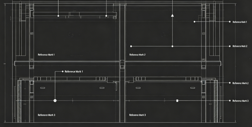
Machine vision cameras capture images of fiducial marks to establish coordinate systems for component placement. Global fiducials on the panel corners allow the equipment to determine the overall position and rotation of the substrate. Local fiducials placed near critical areas or on individual boards provide finer corrections for localized variations. This dual-level approach compensates for material expansion, contraction, or handling-induced shifts that occur between fabrication and assembly stages.
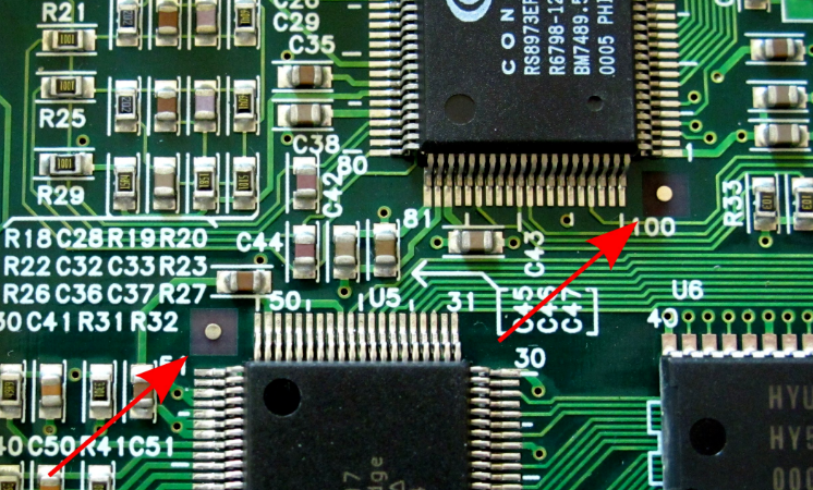
The optical contrast between the fiducial copper and surrounding solder mask or substrate material enables reliable detection under varying lighting conditions. Fiducial placement strategies often include redundant marks to improve robustness against occlusion or damage. PCB panel alignment accuracy depends on the geometric relationship between these marks and the circuit features they reference. Structured engineering analysis of fiducial positioning helps minimize cumulative errors across large panels containing many individual boards.
Fiducial Design Guidelines and Best Practices
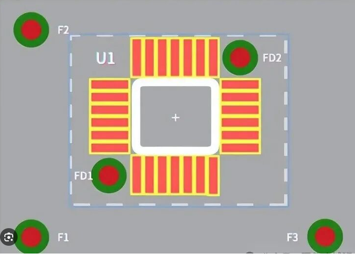
Effective fiducial design begins with selecting shapes that provide clear, rotationally symmetric targets for vision algorithms. Circular marks are commonly preferred because they allow straightforward center-point calculation regardless of orientation. Placement recommendations focus on positioning fiducials at the extremities of the panel while maintaining adequate clearance from routing channels, tooling holes, and board edges. This arrangement maximizes the baseline distance for accurate angle and scale determination.
Designers should ensure that fiducials remain free of solder mask or legend ink that could reduce contrast. Copper-only fiducials with appropriate clearance around them support consistent imaging throughout the manufacturing flow. When multiple boards share a panel, a combination of panel-level and board-level fiducials supports both coarse and fine alignment steps. Following established fiducial design guidelines reduces the likelihood of vision system failures during high-volume SMT runs.
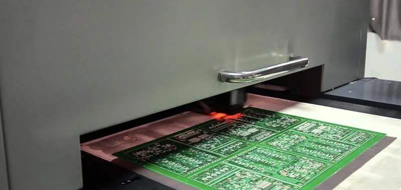
Practical Implementation in PCB Manufacturing
During panelization planning, engineers evaluate panel size, board orientation, and expected thermal profiles to determine optimal fiducial configurations. Redundant fiducials placed diagonally across the panel provide backup references if one mark becomes obscured. Coordination between design and manufacturing teams ensures that fiducial locations align with the capabilities of the specific SMT equipment used downstream. This collaborative approach supports higher first-pass yields and reduces the need for manual intervention.
Troubleshooting alignment issues often starts with verifying fiducial visibility and contrast on production panels. Variations in copper thickness or surface finish can affect detection reliability, prompting adjustments in mark size or surrounding clearance. Consistent application of fiducial placement rules across projects helps standardize processes and simplifies quality control checks. These practices align with broader quality expectations outlined in standards such as IPC-A-600 for board acceptability.
Conclusion
Fiducials provide the foundational reference points that enable precise PCB panel alignment and reliable SMT component placement. Thoughtful application of fiducial design guidelines improves manufacturing consistency while supporting the demands of modern high-density assemblies. By integrating these marks early in the design phase, engineering teams can achieve better registration accuracy and reduced defect rates across panelized production.
FAQs
Q1: What are PCB fiducial marks and how do they support SMT alignment?
A1: PCB fiducial marks are small copper features used as optical targets by automated placement machines. They enable accurate global and local positioning of components on panelized boards. Proper fiducial placement helps compensate for material variations and ensures consistent registration throughout the assembly process.
Q2: How does fiducial placement affect PCB panel alignment?
A2: Strategic fiducial placement at panel corners and key locations allows vision systems to calculate position, rotation, and scale accurately. This supports precise alignment of multiple boards within a single panel during SMT operations. Following established fiducial design guidelines minimizes errors caused by handling or thermal effects.
Q3: What fiducial design guidelines should engineers follow for reliable performance?
A3: Engineers should select high-contrast shapes such as circles and position them to maximize baseline distances while avoiding interference from other features. Adequate clearance around each mark preserves imaging quality. These practices contribute to robust detection across different manufacturing environments.
Q4: Why are fiducials important in high-volume PCB manufacturing?
A4: Fiducials enable automated equipment to maintain tight tolerances even when processing large panels containing many individual boards. They reduce placement variability that could otherwise lead to soldering defects or functional failures. Consistent use of fiducials supports higher throughput and quality in SMT lines.
References
IPC-2221B — Generic Standard on Printed Board Design. IPC, 2012
IPC-A-600K — Acceptability of Printed Boards. IPC, 2020
IPC-7351B — Generic Requirements for Surface Mount Design and Land Pattern Standard. IPC, 2010