 ALLPCB


Electromagnetic interference remains a persistent concern in high-speed electronic designs, where switching signals and external sources can degrade performance or violate regulatory limits. Ferrite components address this challenge by introducing frequency-dependent impedance that attenuates unwanted noise while allowing desired signals to pass. Designers working on printed circuit boards increasingly rely on ferrite beads and cores to meet electromagnetic compatibility goals without compromising board real estate or signal quality. Proper application requires understanding both the material behavior and the circuit topology in which the components operate. This guide outlines the engineering principles, selection criteria, and placement strategies that support effective EMI suppression in PCB layouts.
Why Ferrites Matter for Modern PCB Designs
Ferrite materials exhibit high magnetic permeability combined with significant losses at radio frequencies, converting electromagnetic energy into heat rather than reflecting it back into the circuit. This property makes them suitable for suppressing both conducted and radiated emissions that arise from fast edge rates or long traces acting as antennas. In mixed-signal boards, where digital and analog domains share power and ground planes, uncontrolled noise can couple across sections and affect measurement accuracy or communication reliability. Industry standards such as those in the IEC 61000 series establish test methods and limits that many commercial products must satisfy, driving the need for predictable suppression techniques. Ferrite solutions integrate directly onto the board, offering a compact alternative to larger filter networks when space or cost constraints apply.
Technical Principles and Impedance Behavior
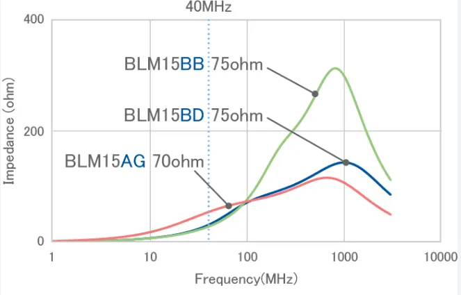
Ferrite impedance rises with frequency because the material transitions from inductive to resistive behavior as magnetic domains respond more slowly to rapid field changes. At lower frequencies the component functions primarily as an inductor, while above a few megahertz the losses dominate and the impedance becomes largely resistive. This characteristic curve allows designers to target specific noise bands without introducing excessive series inductance that could distort lower-frequency signals. Common-mode chokes use paired windings on a shared core to present high impedance to currents flowing in the same direction on multiple lines while presenting low impedance to opposing currents. Differential-mode chokes or single-line ferrite beads address noise that appears between signal and return paths. The distinction matters because common-mode noise often originates from ground potential differences or external fields, whereas differential-mode noise typically stems from switching transients within the circuit itself.
Ferrite Core Selection Considerations
Selection begins with matching the impedance peak to the frequency range of the dominant interference, which is determined through spectrum analysis or simulation of the intended operating environment. Core geometry, material composition, and physical size influence both the magnitude of impedance and the current-handling capability before saturation occurs. Larger cores generally provide higher impedance but occupy more board area and may require additional mechanical support. When multiple noise sources exist, a combination of bead types or a choke followed by beads can achieve broader suppression than any single component. Temperature stability and DC bias effects must also be evaluated, because elevated temperatures or steady currents can shift the impedance curve and reduce effectiveness at the target frequencies. Documentation from material suppliers supplies the necessary curves, yet final validation occurs through prototype measurements on the actual layout.
Placement Techniques for Maximum Effectiveness
Effective suppression depends heavily on locating the ferrite component as close as possible to the noise source or the point where the signal exits the board, such as a connector or cable interface. Placing a bead immediately after a driver minimizes the length of trace that can radiate before the noise is attenuated. For common-mode chokes, the windings must maintain tight coupling and equal lengths to preserve signal integrity while rejecting common-mode currents. Routing traces through or around the core without introducing additional loops prevents the creation of new antenna structures. Power supply lines benefit from beads positioned between the regulator output and the load, particularly when the load contains high-speed switching elements. Ground planes should remain continuous beneath the component to avoid creating slots that could increase radiated emissions.
Best Practices in PCB Layout and Integration
Designers achieve consistent results by treating ferrite components as part of an overall filtering strategy rather than isolated fixes. Decoupling capacitors placed on either side of a bead help form a low-pass network that further attenuates high-frequency content. When using multiple beads on the same net, spacing them apart prevents magnetic coupling that could reduce overall effectiveness. Thermal reliefs around the component pads should be evaluated because excessive copper removal can increase series resistance and alter the intended impedance. In dense layouts, orientation of the core relative to nearby traces or other magnetic components influences crosstalk; aligning the core axis perpendicular to adjacent current paths often reduces unwanted coupling. Verification through near-field probing or conducted emission scans on early prototypes confirms that the chosen configuration meets the required margins before committing to production tooling.
Conclusion
Ferrites provide a practical, board-level method for controlling EMI when selected and placed according to the frequency content of the noise and the topology of the circuit. Understanding the transition from inductive to resistive impedance, distinguishing common-mode from differential-mode suppression, and applying consistent placement rules enable designers to achieve compliance with electromagnetic compatibility requirements while preserving signal integrity. Integration with surrounding decoupling and grounding practices further enhances performance. Systematic measurement on prototypes remains the final step that validates the design choices.
FAQs
Q1: How do ferrite beads contribute to EMI suppression on PCBs?
A1: Ferrite beads introduce frequency-selective impedance that attenuates high-frequency noise while passing lower-frequency signals with minimal distortion. Proper selection based on the target interference spectrum and placement close to noise sources or board interfaces maximizes their effectiveness in reducing both conducted and radiated emissions.
Q2: What factors guide ferrite core selection for common-mode chokes?
A2: Core material, geometry, and impedance characteristics must align with the frequency range of common-mode noise, the expected current levels, and available board space. Evaluation of saturation behavior under DC bias and temperature variations ensures reliable performance across operating conditions.
Q3: Where should designers position ferrite components for best results?
A3: Components perform optimally when located immediately adjacent to noise-generating circuits or at cable entry and exit points. Maintaining short trace lengths after the ferrite and preserving continuous return paths prevents the formation of additional radiating structures.
Q4: How do differential-mode and common-mode chokes differ in application?
A4: Differential-mode chokes or beads target noise appearing between a signal line and its return, while common-mode chokes address currents flowing in the same direction on multiple conductors. The choice depends on whether the dominant interference originates from internal switching or external fields and ground potential differences.
References
IEC 61000 series — Electromagnetic compatibility (EMC). IEC
IPC-2221B — Generic Standard on Printed Board Design. IPC, 2012
ISO 9001:2015 — Quality Management Systems. ISO, 2015


