 ALLPCB


Introduction
Printed circuit boards experience various mechanical stresses during manufacturing and assembly that can lead to deformation known as the PCB potato chip effect. This phenomenon occurs when a PCB warps into a curved shape resembling a potato chip, primarily due to uneven internal stresses from asymmetric material properties or copper distribution. For electric engineers designing high-layer-count boards, recognizing this issue early is crucial to ensure reliability in applications like telecommunications and automotive electronics. Warpage compromises solder joint integrity, misaligns components during surface mount technology processes, and increases failure rates in the field. By understanding the root causes and implementing copper balancing solutions, designers can significantly reduce these risks. This article explores the mechanisms behind PCB warpage and provides practical PCB design guidelines for prevention.
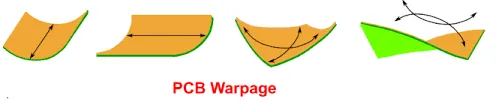
What Is the PCB Potato Chip Effect and Why Does It Matter?
The PCB potato chip effect specifically refers to a type of warpage where the board bows convexly or concavely across its plane, often triggered by thermal cycling during lamination or reflow soldering. This deformation, also called bow or twist, exceeds acceptable limits when it surpasses 0.75% of the board's diagonal length for surface-mount assemblies, as outlined in industry standards. Engineers must prioritize PCB warpage prevention because even minor distortions disrupt automated pick-and-place operations, leading to stencil misalignment and bridging defects. In multilayer boards, this effect amplifies reliability concerns, such as delamination or cracking under vibration. Ignoring it results in higher rework costs and delayed time-to-market. Addressing it through symmetrical PCB stackup and copper balancing ensures consistent performance across production runs.
Causes of PCB Warpage: The Role of Thermal Expansion and Material Asymmetry
PCB warpage stems from differential coefficients of thermal expansion (CTE) between copper and the laminate substrate, such as FR-4, which expands more during heating. Copper, with a lower CTE around 17 ppm/°C compared to FR-4's 15-20 ppm/°C in the z-axis, contracts unevenly if distribution is imbalanced, creating internal stresses. During lamination at temperatures above 170°C, these stresses lock in, manifesting as the potato chip effect upon cooling. Asymmetric stackups exacerbate this, where outer layers have heavier copper pours while inner layers remain sparse. Moisture absorption further worsens the issue by causing additional expansion during reflow peaks at 260°C. Pattern density variations, like concentrated power planes on one side, compound these forces, leading to predictable deformation patterns.
Manufacturing factors like uneven pressing during lamination or improper cooling rates contribute, but design choices dominate. Engineers observe that boards with copper coverage differing by more than 10-15% between layers show pronounced warpage. High-layer counts, common in modern designs exceeding 12 layers, heighten vulnerability due to cumulative asymmetries. Without intervention, these boards fail flatness specifications, impacting impedance control and signal integrity. Proactive analysis during the design phase identifies hotspots before fabrication. Understanding these mechanisms allows for targeted PCB warpage prevention strategies.
Technical Principles Behind Copper Imbalance and Warpage
Copper balancing addresses the core issue of uneven etch factors and plating stresses by ensuring uniform copper density across each layer and symmetry between opposing layers. In an ideal setup, each signal layer pairs with a similar plane layer at equal distance from the board's neutral axis, minimizing net torque from thermal expansion. The neutral axis, typically at the board's center, serves as the reference where stresses cancel out in a balanced structure. Deviations cause one side to dominate, pulling the board into the potato chip shape. Finite element analysis tools simulate these behaviors, predicting warpage based on layer thicknesses and copper percentages. Maintaining 40-60% copper fill per layer, adjusted for functionality, proves effective in practice.
Resin distribution plays a supporting role, as unbalanced copper leaves excess resin on sparse areas, altering local CTE. During high-temperature processes, this mismatch generates hygroscopic stresses, amplifying bow. Standards like IPC-TM-650 method 2.4.22 quantify bow and twist by measuring diagonal deviations under controlled conditions. Engineers apply these principles by mirroring layer configurations, such as signal-ground-signal pairs around the core. This approach not only curbs warpage but also stabilizes dielectric constants for better signal performance. Consistent application yields boards within 0.5% flatness, surpassing typical requirements.
Copper Balancing Solutions: Key PCB Design Guidelines
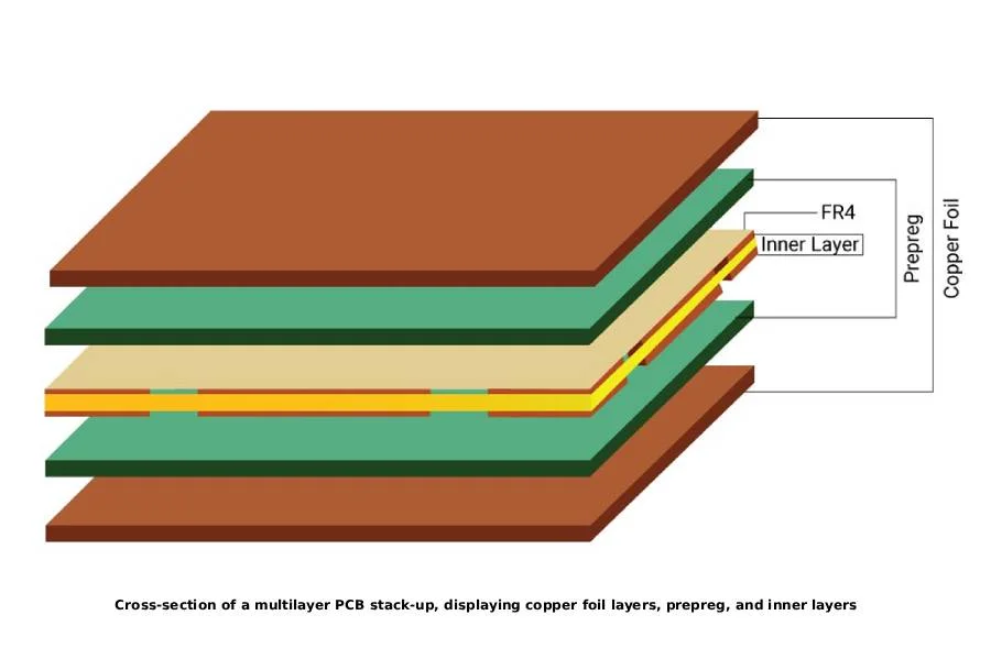
Effective copper balancing solutions begin with layout strategies that distribute traces, pours, and planes evenly within each layer. Designers add copper thieves or dummy fills in low-density regions, ensuring no area exceeds a 15% density gradient from the average. For power and ground planes, partial etching or grid patterns prevent solid blocks that overpower adjacent signal layers. These grids maintain electrical continuity while reducing effective copper mass, promoting balance. Symmetrical PCB stackup demands mirroring: layer 1 matches layer n, layer 2 matches layer n-1, and so on, with the core providing rigidity. Avoiding hybrid materials with disparate CTEs further supports this.
During routing, alternate trace directions between layers to equalize etch imbalances from directional plating. Board shape influences warpage; rectangular panels with uniform borders minimize edge effects compared to irregular cutouts. Simulate stackups early using vendor DFM feedback to iterate on copper percentages. For high-reliability boards, target under 50% overall copper asymmetry. These PCB design guidelines integrate seamlessly into workflows, preventing the potato chip effect without compromising functionality. Validation through shadow moiré or dial gauge tests confirms compliance post-fabrication.
Best Practices for Symmetrical PCB Stackup and Manufacturing Considerations
Implement a symmetrical PCB stackup by selecting core thicknesses that center the build, typically 0.8-1.6 mm for 8-16 layer boards. Pair heavy copper layers oppositely, using 1 oz/ft2 signal layers balanced by 0.5-1 oz planes. Prepreg selection with matched resin content ensures uniform flow during lamination, reducing voids that induce stress. Bake bare boards at 125°C for 4-6 hours to expel moisture before assembly, mitigating reflow warpage spikes. Panelization with 20-50% border copper and v-scoring alignment distributes forces evenly across arrays.
Collaborate with fabricators for stackup reviews, specifying copper balance targets in fab notes. For fine-pitch BGAs, tighten warpage specs to 0.5% via IPC-A-600 criteria. Post-lamination flattening via fixtures or controlled cooling aids recovery, though design prevention outperforms remediation. These practices yield robust boards resilient to thermal excursions. Engineers adopting them report fewer assembly rejects and enhanced long-term reliability.
Advanced Troubleshooting: Analyzing and Correcting Warpage in Designs
When warpage appears in prototypes, dissect the stackup for copper density variances using layer reports from design software. Compare top-bottom asymmetries first, then intra-layer gradients. Adjust by flooding sparse zones with hatched fills, verifying impedance impacts. If stackup asymmetry persists, rebuild around a thicker core or thin outer layers symmetrically. Thermal profiling during reflow simulates real stresses, guiding material tweaks like higher Tg laminates above 170°C.
Case insights reveal that boards with peripheral copper frames resist edge curling better than unframed ones. For HDI designs, microvia stacking must mirror to avoid z-axis imbalances. Iterative DFM loops refine these, often resolving 80% of issues pre-production. Document lessons in design libraries for reuse. This structured approach turns warpage challenges into optimized solutions.
Conclusion
The PCB potato chip effect arises from copper imbalances and asymmetric stackups that induce thermal stresses, but copper balancing solutions offer reliable prevention. Symmetrical PCB stackup, uniform density fills, and adherence to PCB design guidelines ensure flatness within industry tolerances. Electric engineers benefit from early simulation and DFM integration to avoid assembly pitfalls and reliability failures. Implementing these strategies minimizes risks across multilayer designs. Prioritizing balance from concept to fabrication delivers high-yield, durable boards ready for demanding applications.
FAQs
Q1: What is the PCB potato chip effect?
A1: The PCB potato chip effect describes warpage where a board curves like a potato chip due to uneven copper distribution and CTE mismatches during thermal processes. This deformation stresses solder joints and hinders SMT assembly. Prevention focuses on copper balancing solutions and symmetrical PCB stackup to maintain flatness under 0.75% bow or twist.
Q2: How can engineers implement PCB warpage prevention through copper balancing?
A2: Start by targeting 40-60% copper density per layer with thieves in sparse areas and mirrored stackups around the neutral axis. Use grid patterns on planes to equalize mass without full solids. These PCB design guidelines reduce internal stresses from lamination and reflow, ensuring compliance with flatness specs.
Q3: Why is symmetrical PCB stackup critical for multilayer boards?
A3: Symmetrical PCB stackup mirrors layers to cancel thermal expansion torques, preventing the potato chip effect in high-layer counts. It stabilizes the neutral axis, minimizes resin imbalances, and supports signal integrity. Designers pair signal-ground layers oppositely for optimal PCB warpage prevention.
Q4: What role do industry standards play in PCB warpage control?
A4: Standards define acceptable limits and test methods, guiding copper balancing solutions. They ensure designs meet bow and twist thresholds for reliable assembly. Following them integrates seamlessly into PCB design guidelines for consistent quality.
References
IPC-A-600K — Acceptability of Printed Boards. IPC, 2020
IPC-6012E — Qualification and Performance Specification for Rigid Printed Boards. IPC, 2017
IPC-TM-650 2.4.22 — Bow and Twist. IPC, 2015


