 ALLPCB


Introduction
In the demanding world of automotive electronics manufacturing, printed circuit boards (PCBs) must deliver exceptional reliability under extreme conditions like vibration, temperature fluctuations, and high-speed data transmission. Controlled depth drilling emerges as a critical technique to meet these challenges by enabling precise via formation without penetrating the entire board stackup. This method supports higher interconnect densities essential for modern automotive systems such as advanced driver-assistance systems (ADAS) and powertrain controls. By optimizing via stub lengths, controlled depth drilling enhances signal integrity in automotive applications, reducing crosstalk and insertion loss. Automotive PCB drilling techniques like this directly contribute to reliable PCB design, ensuring compliance with rigorous performance standards. As vehicles evolve toward electrification and autonomy, mastering controlled depth drilling applications becomes vital for engineers focused on long-term durability.
What Is Controlled Depth Drilling and Why It Matters in Automotive Electronics
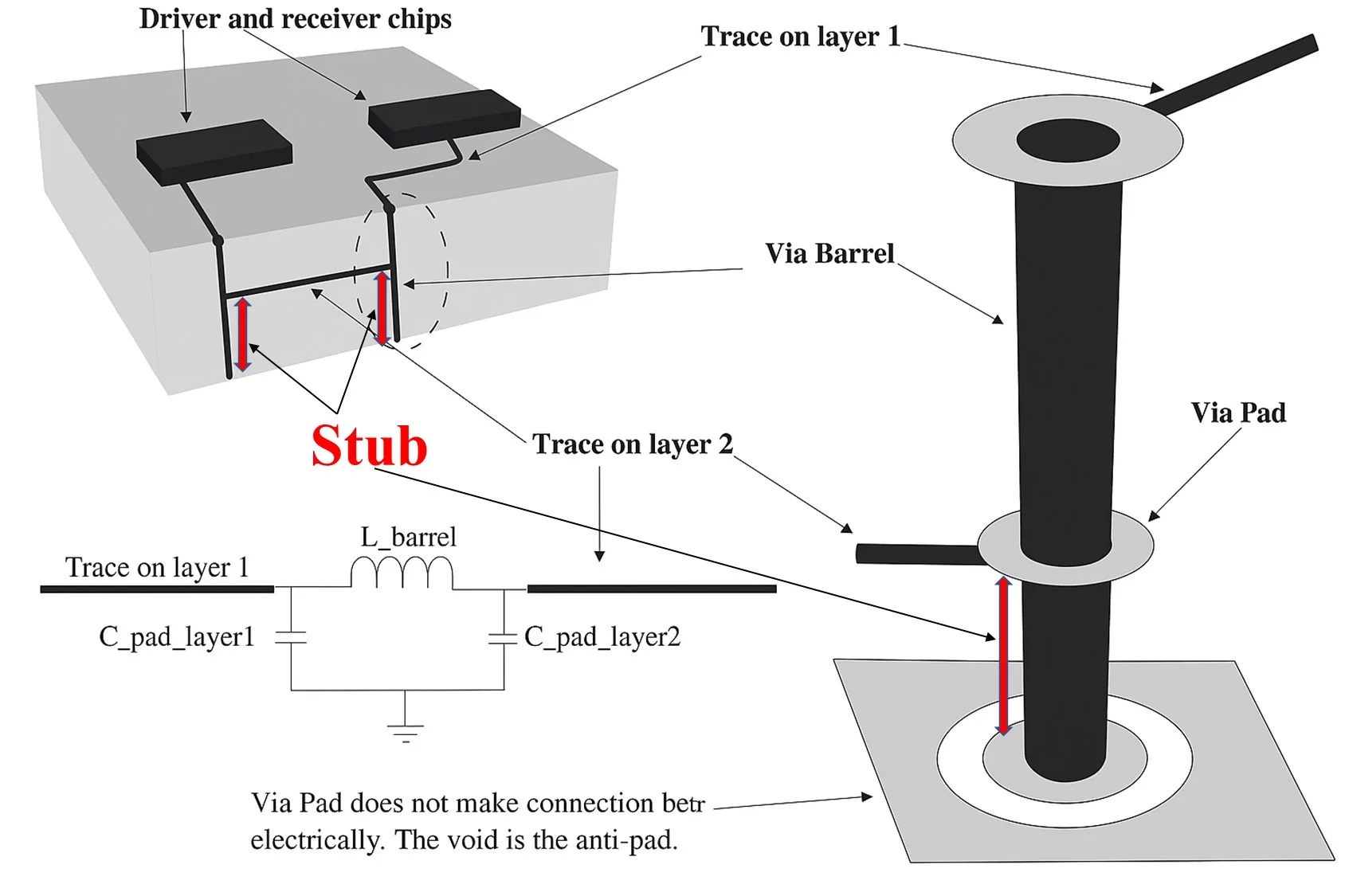
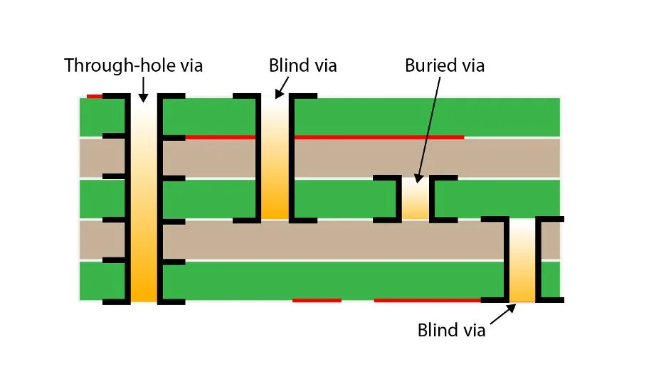
Controlled depth drilling refers to a PCB fabrication process where holes are drilled to a predetermined depth, creating blind or buried vias that stop short of the opposite board surface. Unlike standard through-hole drilling, this technique requires exact control over drill penetration to avoid damaging inner layers or creating unwanted stubs that degrade electrical performance. In automotive electronics manufacturing, where PCBs handle high-frequency signals up to several gigahertz, minimizing via stubs is crucial for maintaining signal integrity automotive standards demand. This process allows for denser routing in multilayer boards, accommodating the compact designs needed for engine control units, sensor interfaces, and infotainment systems.
The relevance stems from automotive environments exposing PCBs to thermal cycling from -40°C to 125°C, mechanical stresses, and electromagnetic interference. Poorly controlled drilling can lead to via breakout, resin smear, or inconsistent depths, compromising reliable PCB design and potentially causing intermittent failures in safety-critical systems. Controlled depth drilling applications enable finer pitch vias, supporting the transition to high-density interconnect (HDI) structures prevalent in electric vehicle power electronics. Factory insights reveal that precise depth control reduces rework rates and improves yield, aligning with quality benchmarks in production lines. Ultimately, this technique optimizes overall PCB performance, ensuring automotive systems operate flawlessly over extended lifecycles.
Technical Principles of Controlled Depth Drilling
The core principle of controlled depth drilling involves synchronizing spindle speed, feed rate, and depth sensors to achieve target penetration within microns. Mechanical systems use peck drilling cycles, where the tool retracts periodically to clear chips and measure progress via optical encoders or laser interferometers. Laser-based methods employ ablation with excimer or UV lasers, offering sub-micron accuracy for microvias under 100 microns in diameter, ideal for high-speed automotive signals. Depth tolerance typically ranges from ±10% to ±25% of nominal depth, depending on board thickness and material stackup, to prevent inner layer damage.
Material interactions play a key role, as drill bits encounter varying resistances from copper foils, prepregs, and cores. In epoxy-based laminates common in automotive PCBs, heat generation during drilling must be managed to avoid delamination or fiberglass protrusion. Process parameters like thrust force and chip load are optimized through empirical testing to balance speed and precision. Adherence to IPC-6012E standards ensures via geometry meets qualification criteria for rigid boards, including annulus dimensions and plating uniformity. These principles underpin reliable PCB design by enabling consistent electrical characteristics across production batches.
Signal propagation benefits significantly, as shorter vias reduce inductive and capacitive parasitics. For automotive PCB drilling, this translates to lower return loss in differential pairs used for CAN bus or Ethernet interfaces. Engineers must model stackups using field solvers to predict depth impacts on impedance, guiding drill parameter selection.
Controlled Depth Drilling Applications in Automotive Electronics
In engine control modules, controlled depth drilling facilitates stacked microvias for power and ground planes, minimizing inductance in switched-mode power supplies. These applications support high current densities required for ignition coils and fuel injectors, while preserving space for surface-mount components. For ADAS radar and camera modules, blind vias connect high-speed SerDes lanes directly to inner signal layers, enhancing signal integrity automotive performance under vibration.
Infotainment systems leverage buried vias drilled to exact depths for HDMI and LVDS interfaces, reducing crosstalk in dense routing channels. Automotive electronics manufacturing benefits from this by enabling thinner boards without sacrificing layer count, crucial for under-hood placements. Battery management systems in electric vehicles use controlled depth drilling for isolated sense lines, preventing shorts in high-voltage environments. These targeted applications demonstrate how the technique drives miniaturization and efficiency.
Reliable PCB design in telematics units relies on uniform via depths to maintain timing margins for GPS and cellular modems. Factory processes integrate depth verification via automated X-ray or electrical testing post-drilling. Overall, controlled depth drilling applications expand design flexibility, aligning with the push for more integrated, performant automotive electronics.
Best Practices for Implementing Controlled Depth Drilling in Production
Start with thorough stackup planning, defining via depths based on layer pairings and simulating signal paths for integrity. Select drill types suited to materials: carbide for mechanical macro-vias over 150 microns, CO2 lasers for deeper blind vias in thick cores. Implement entry and exit material on panels to protect surfaces, and use registration fiducials for multilayer alignment during sequential drilling.
Process control involves real-time monitoring with depth gauges and peck cycles adjusted for board warpage. Post-drill inspection per IPC-A-600K criteria checks for breakout, smear, and plating voids using cross-sectioning samples. Desmear processes like plasma or permanganate etching ensure clean barrel walls before electroless copper deposition. Engineers should qualify tools through drill hit counts, targeting 10,000 to 50,000 hits per bit based on diameter.
In automotive PCB drilling workflows, integrate statistical process control to track depth variation across panels. Collaborate with fabricators early to match design rules to equipment capabilities, such as maximum depth-to-diameter ratios of 10:1. These practices yield robust boards resilient to automotive stresses.
Challenges and Troubleshooting in Automotive PCB Drilling
Common issues include drill wander in thin cores, leading to oversized holes and impedance mismatches. Mitigate by using pilot drills or straight-flute bits with high helix angles for better chip evacuation. Thermal expansion during multi-step drilling can shift depths; compensate with temperature-controlled fixtures and sequential lamination.
Resin smear on inner layers disrupts plating adhesion, addressed via optimized feed rates and chemical desmear. In high-volume automotive electronics manufacturing, tool wear accelerates inconsistencies; schedule replacements based on footage drilled. Vibration from sequential builds may cause misalignment, countered by precise panel sizing and optical registration.
Troubleshooting starts with failure analysis: microsections reveal depth errors, while flying probe tests detect opens. Adjust parameters iteratively, documenting changes for process refinement. These strategies ensure controlled depth drilling applications deliver reliable PCB design outcomes.
Conclusion
Controlled depth drilling stands as a cornerstone for advancing PCB performance in automotive electronics, enabling compact, high-reliability designs critical for next-generation vehicles. By precisely managing via depths, it bolsters signal integrity automotive requirements and supports denser interconnects without compromising durability. Factory-driven best practices, grounded in standards like IPC-6012E and IPC-A-600K, guide implementation for consistent results. Engineers adopting these techniques can optimize automotive PCB drilling processes, fostering innovation in reliable PCB design. As automotive systems grow more complex, controlled depth drilling applications will remain indispensable for meeting performance and safety demands.
FAQs
Q1: What are the primary benefits of controlled depth drilling in automotive PCB drilling?
A1: Controlled depth drilling creates blind and buried vias that shorten signal paths, improving signal integrity automotive by reducing stubs and parasitics. It enables higher layer counts in compact boards for ADAS and power electronics, enhancing density without through-hole interference. Factories achieve better yields through precise depth control, aligning with reliable PCB design needs in harsh environments. This technique supports high-frequency operation essential for modern vehicles.
Q2: How does controlled depth drilling impact signal integrity automotive applications?
A2: In automotive electronics manufacturing, controlled depth drilling minimizes via stubs, lowering insertion loss and crosstalk for interfaces like Ethernet and radar. Shorter vias maintain controlled impedance, crucial for data rates exceeding 10 Gbps in infotainment. Depth accuracy prevents reflections that degrade eye diagrams. Engineers verify via TDR testing post-fabrication for compliance. Overall, it ensures robust performance under thermal and mechanical stresses.
Q3: What standards guide controlled depth drilling applications in reliable PCB design?
A3: IPC-6012E specifies performance for rigid boards, including via geometry tolerances critical for automotive use. IPC-A-600K defines acceptability criteria for drilled holes, such as no breakout beyond specified annuli. These standards ensure depth control meets automotive reliability thresholds. Factories reference them during qualification to standardize processes. Adherence minimizes field failures in electronics manufacturing.
Q4: What are best practices for troubleshooting depth variations in automotive PCB drilling?
A4: Monitor spindle feedback and peck cycles to detect wander early, adjusting feed rates for material types. Use X-ray laminography for non-destructive depth checks on production panels. Cross-section samples confirm tolerances per IPC guidelines. Optimize chip load to prevent smear affecting plating. Iterative tooling qualification stabilizes processes for consistent reliable PCB design.
References
IPC-6012E — Qualification and Performance Specification for Rigid Printed Boards. IPC, 2017
IPC-A-600K — Acceptability of Printed Boards. IPC, 2020


