 ALLPCB


Introduction
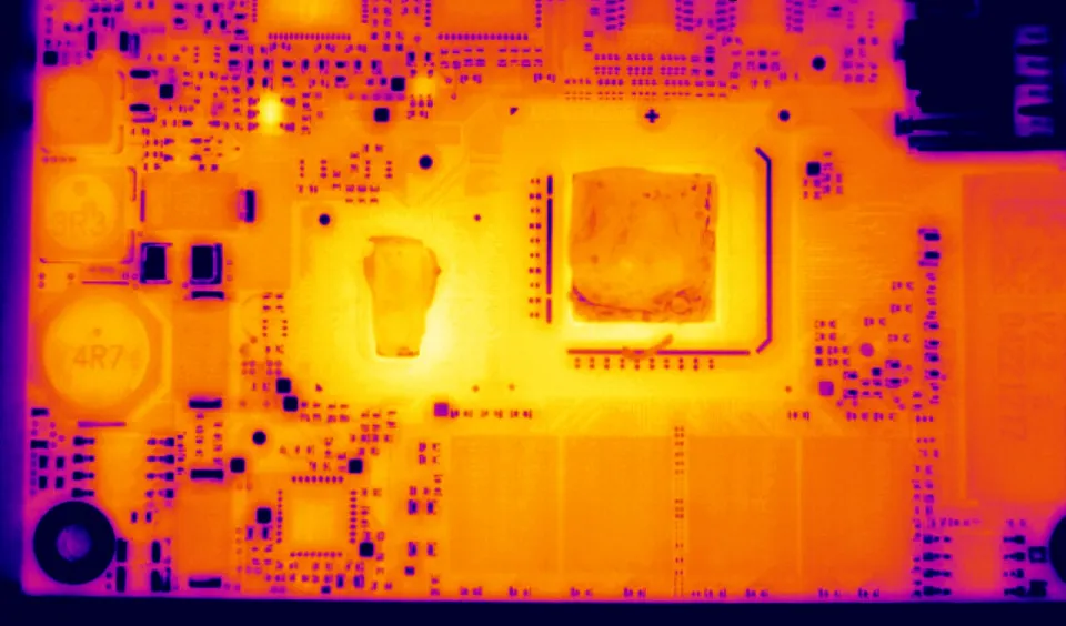
Thermal runaway poses a critical threat in modern PCB designs, particularly in high-power applications where components generate excessive heat. This phenomenon occurs when rising temperatures trigger increased current flow, leading to further heating and potential failure. Effective PCB thermal management is essential to mitigate these risks and ensure long-term PCB reliability. Copper balancing emerges as a key strategy in this context, promoting uniform heat dissipation across the board. By addressing copper distribution asymmetries, engineers can prevent hotspots that accelerate component degradation. This approach not only enhances hotspot prevention in PCBs but also extends component lifespan in demanding environments.
Understanding Thermal Runaway in PCBs
Thermal runaway in PCBs refers to a self-reinforcing cycle where heat buildup causes components to operate beyond safe limits, resulting in exponential temperature increases. Power devices like MOSFETs, voltage regulators, and LEDs are particularly susceptible due to their inherent positive temperature coefficients. Poor heat dissipation exacerbates this, creating localized hotspots that compromise solder joints and insulation materials. The consequences extend to reduced component lifespan on PCBs and overall system unreliability, often manifesting as intermittent failures or catastrophic shorts. Industry standards such as IPC-6012E emphasize the need for designs that maintain structural integrity under thermal stress, underscoring why proactive thermal strategies matter.
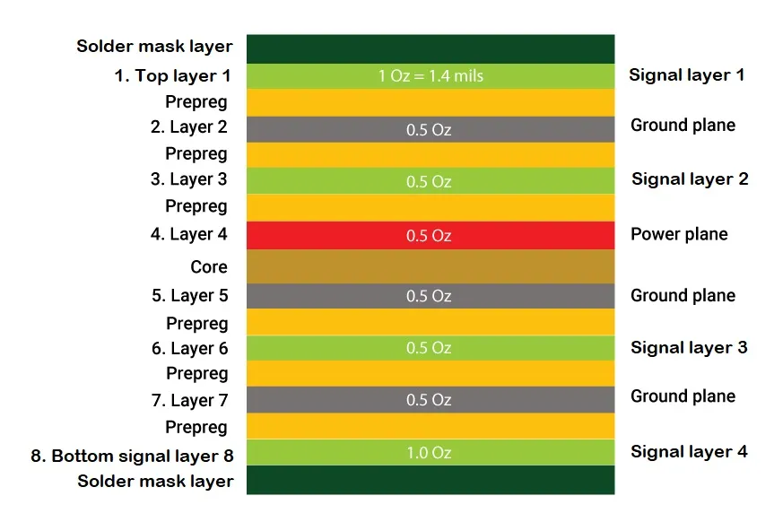
Engineers must recognize that thermal runaway often stems from inadequate heat paths rather than just high ambient conditions. In multilayer boards, uneven heat distribution can propagate through layers, affecting adjacent components. This not only shortens operational life but also increases failure rates in field deployments. Addressing these issues through targeted PCB thermal management techniques directly bolsters reliability metrics.
The Impact of Copper Distribution on Heat Dissipation
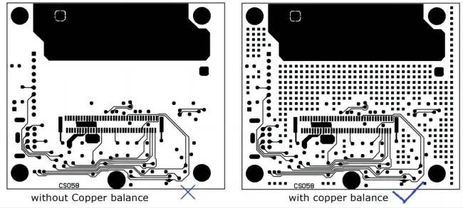
Copper serves as the primary thermal conductor in PCBs, with its high conductivity enabling efficient heat spreading from active components. However, imbalanced copper areas across layers lead to uneven thermal paths, concentrating heat in densely routed sections. This imbalance arises during design when signal traces dominate one side while ground planes occupy the other, creating asymmetric expansion during lamination. Balanced copper distribution counters this by ensuring uniform conductivity, which aids in hotspot prevention for PCBs. Consequently, copper balancing for heat dissipation becomes integral to robust thermal management.
In practice, uneven copper not only induces mechanical warpage but also thermal gradients that elevate junction temperatures. These gradients can push components toward thermal runaway thresholds, especially under sustained loads. Standards like IPC-A-600K provide guidelines for acceptable board flatness, indirectly supporting thermal uniformity by minimizing stress-induced voids in heat paths. Engineers benefit from viewing copper balancing as a dual-purpose technique for both mechanical and thermal stability.
Mechanisms Linking Copper Imbalance to Hotspots and Runaway
Uneven copper distribution creates regions of high thermal resistance, where heat from power components fails to spread effectively. Dense copper areas act as sinks, pulling heat away from sparse regions and forming hotspots elsewhere. This localized overheating increases trace resistance, amplifying I2R losses and perpetuating the cycle toward thermal runaway. In multilayer stacks, interlayer imbalances worsen via thermal coupling, where heat tunnels through poorly balanced planes.
Warpage from copper asymmetry further complicates dissipation by altering contact interfaces and airflow over the board. Components mounted on warped surfaces experience inconsistent thermal coupling, accelerating fatigue in solder joints. Copper balancing mitigates these by promoting symmetric expansion coefficients across layers, as aligned with IPC-6012E performance specs. The result is a more predictable thermal profile, enhancing component lifespan on PCBs.
Best Practices for Copper Balancing in PCB Design
Start copper balancing by calculating copper coverage per layer during the layout phase, aiming for 50-70% uniformity across top, bottom, and inner planes. Use fill patterns or dummy patterns in low-density areas to match opposing layers without altering electrical performance. For power sections, integrate solid planes symmetrically while incorporating thermal vias to bridge layers effectively. This approach optimizes copper balancing for heat dissipation, directly supporting PCB thermal management goals.
Validate balance through stackup reviews, ensuring outer layers mirror each other in weight. In high-current designs, thicker copper on balanced planes reduces resistive heating per IPC-2152B guidelines for current capacity. Avoid overfilling edges to prevent plating inconsistencies during fabrication. These steps collectively prevent hotspots and bolster PCB reliability.
Integrating Copper Balancing with Other Thermal Strategies
Combine copper balancing with via arrays under hotspots to create vertical heat conduits, enhancing overall dissipation in dense boards. Strategic component placement away from edges leverages balanced planes for lateral spreading. For multilayer PCBs, alternate signal and plane layers symmetrically to maintain thermal equity. This holistic method extends beyond basic balancing, addressing complex heat flows in high-reliability applications.
Monitor potential interactions like EMI from large pours by segmenting them judiciously. In power electronics, balanced heavy copper layers handle elevated currents while distributing heat evenly, averting runaway risks. Regular design rule checks ensure compliance, yielding boards with superior thermal margins.
Case Insights: Troubleshooting Thermal Issues
Consider a scenario where a power supply PCB exhibited recurrent failures under load. Analysis revealed top-layer dominance in copper due to routing, causing bottom-layer hotspots and warpage. Implementing balancing via added ground fills resolved the issue, stabilizing temperatures and eliminating intermittent drops. Such cases highlight how copper imbalance masquerades as other faults, underscoring the need for early intervention.
Similar patterns appear in automotive modules, where vibration amplifies warpage effects on thermal paths. Balanced designs consistently show improved endurance, aligning with reliability demands.
Conclusion
Copper balancing stands as a foundational element in combating thermal runaway through superior PCB thermal management. By ensuring even heat dissipation and hotspot prevention in PCBs, it safeguards component lifespan and elevates overall reliability. Engineers should prioritize symmetric copper distribution in stackups, guided by established standards. Adopting these practices yields robust designs capable of withstanding real-world thermal stresses, minimizing failures and extending service life.
FAQs
Q1: What is copper balancing and its role in PCB thermal management?
A1: Copper balancing involves symmetric copper distribution across PCB layers to prevent warpage and ensure uniform heat spreading. This technique enhances PCB thermal management by minimizing thermal gradients and hotspots. Uneven copper creates resistance variations that concentrate heat, risking component damage. Proper balancing aligns with fabrication best practices for reliable heat dissipation.
Q2: How does copper balancing prevent hotspots in PCBs?
A2: Hotspot prevention in PCBs relies on copper balancing to distribute thermal conductivity evenly, avoiding localized overheating. Imbalanced layers form high-resistance zones where heat accumulates, accelerating degradation. Balanced pours act as spreaders, channeling heat to board edges or sinks. This directly supports PCB reliability in power-intensive designs.
Q3: Can copper balancing improve component lifespan on PCBs?
A3: Yes, copper balancing extends component lifespan on PCBs by maintaining lower, uniform operating temperatures through effective heat dissipation. Hotspots from imbalances cause thermal cycling that fatigues materials and joints. Symmetric distribution reduces these stresses, preventing premature failures. It complements other strategies for enhanced longevity.
Q4: What standards guide copper balancing for thermal performance?
A4: Standards like IPC-6012E specify flatness requirements that support copper balancing for thermal uniformity. IPC-A-600K addresses acceptability criteria for balanced boards under stress. These ensure designs resist warpage-induced thermal issues, promoting reliable heat paths. Adherence optimizes PCB thermal management outcomes.
References
- IPC-6012E — Qualification and Performance Specification for Rigid Printed Boards. IPC, 2018
- IPC-A-600K — Acceptability of Printed Boards. IPC, 2020
- IPC-2152B — Standard for Determining Current Carrying Capacity in Printed Board Design. IPC, 2009


