 ALLPCB


Introduction
Multi-layer printed circuit boards form the backbone of modern electronics, enabling compact designs with high interconnect density. As electronic devices demand more functionality in smaller footprints, the multi-layer PCB fabrication process becomes increasingly complex. Sequential lamination emerges as a critical technique in this domain, allowing manufacturers to construct boards with blind and buried vias that standard methods cannot achieve. This process builds the board through multiple lamination cycles, offering precise control over layer integration. For electric engineers, understanding sequential lamination unlocks opportunities to optimize PCB layer stackup design for performance and reliability. Factory insights reveal its role in producing high-density interconnect boards essential for telecommunications and computing applications.
What Is Sequential Lamination?
Sequential lamination refers to a multi-layer PCB fabrication process where the board is assembled through successive lamination steps using pre-laminated subcomposites or cores. Unlike traditional multi-layer production, which laminates all inner layers simultaneously, this method adds layers incrementally, often inserting dielectric materials between copper foils and existing sub-stacks. Each cycle involves processing, drilling, plating, and bonding, enabling features like blind vias that connect only adjacent layers. This approach suits high-layer-count boards exceeding eight layers, where uniformity across cycles is paramount. Engineers appreciate its flexibility in accommodating asymmetric stackups while maintaining structural integrity. In practice, it supports the creation of complex interconnects vital for signal integrity in dense designs.
Why Sequential Lamination Matters in Multi-Layer PCB Fabrication
Sequential lamination addresses limitations in standard fabrication by enabling higher routing densities and reduced via stubs, which improve electrical performance. It allows for buried vias that conserve surface space, crucial for high-speed signals where impedance control is key. Factory-driven perspectives highlight its necessity for boards with 20 or more layers, where single-cycle lamination risks warpage or delamination. By breaking the process into stages, manufacturers gain better yield control and adaptability to material variations. For electric engineers designing PCB layer stackup, this method influences choices in via types and layer pairing, directly impacting thermal management and mechanical stability. Ultimately, it elevates the multi-layer PCB fabrication process to meet demands of advanced applications like servers and automotive electronics.
The Sequential Lamination Process Flow
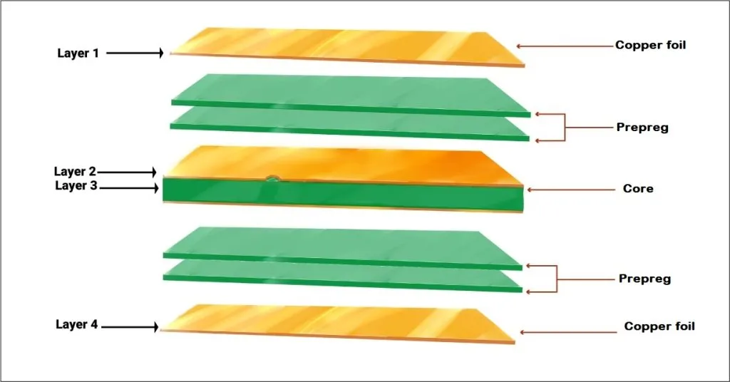
The sequential lamination process flow begins with fabricating inner layer cores, typically pairs like layers 2-3 or 5-6, following standard imaging and etching procedures. These cores are then laminated to outer copper foils using prepreg sheets under controlled heat and pressure to form a sub-composite. Blind vias are drilled into specific layers, electroplated to establish interconnections, and the surface prepared for additional layering. This sub-stack is registered precisely before the next lamination cycle, where more prepregs and foils are added, repeating the drill-plate-laminate sequence. Final outer layers receive imaging, plating for through-holes, and surface finishes. Throughout, material flow consistency ensures void-free bonds, as emphasized in IPC-4101 specifications for base materials in multi-cycle processes.
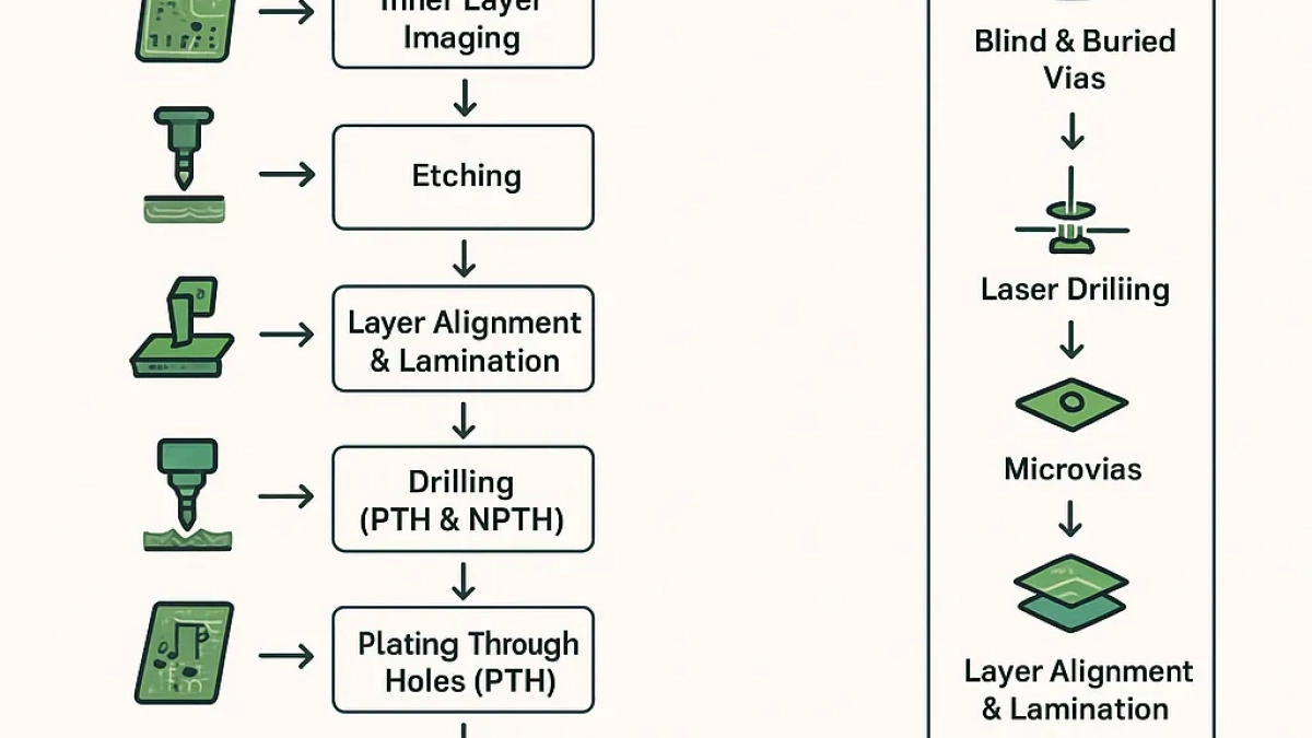
Alignment fiducials guide each step to prevent misalignment, which could compromise via reliability. Press cycles operate at temperatures around glass transition points of resins, balancing flow and adhesion. Post-lamination inspections verify thickness uniformity and continuity. This iterative flow distinguishes sequential lamination, making it ideal for the multi-layer PCB fabrication process in high-density builds.
PCB Layer Stackup Design Considerations for Sequential Lamination
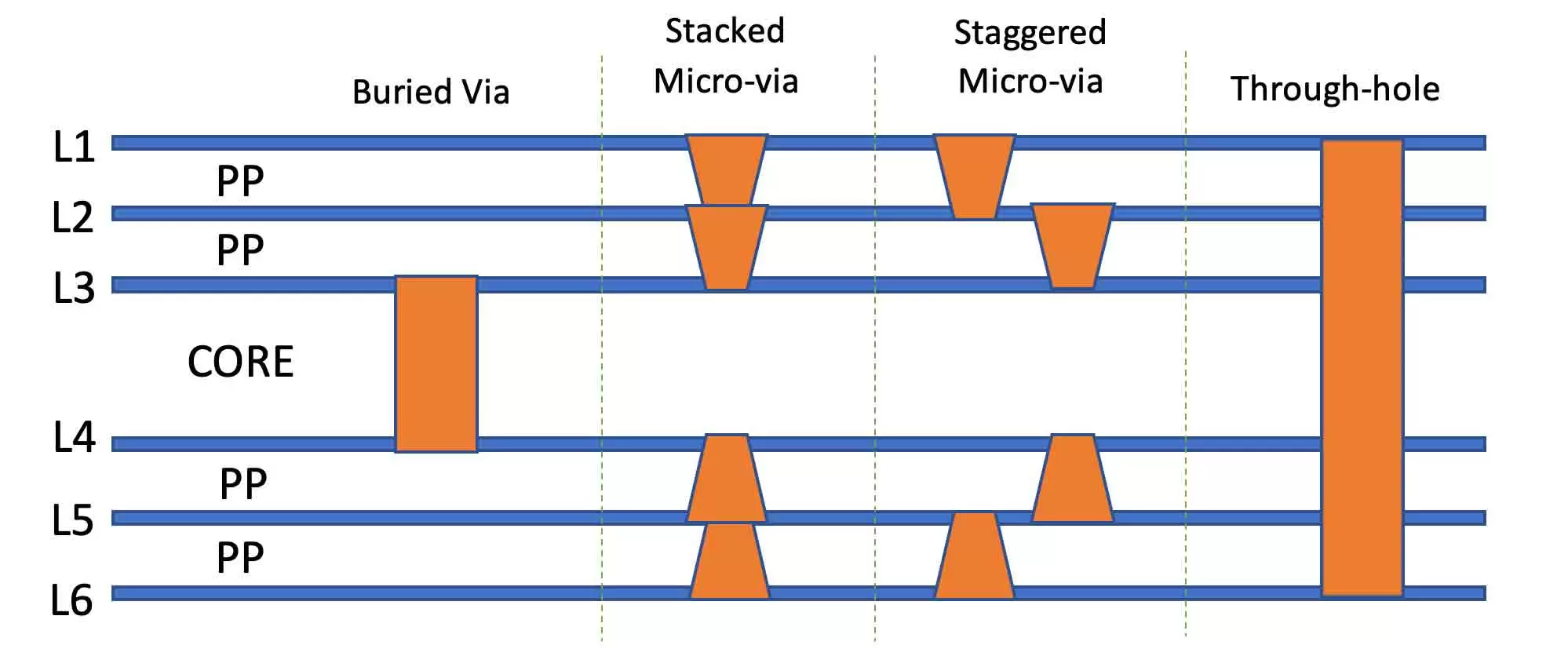
Effective PCB layer stackup design in sequential lamination prioritizes symmetry to minimize warpage, pairing signal layers with ground or power planes on both sides of the neutral axis. Engineers must specify core and prepreg thicknesses that match across cycles, ensuring consistent dielectric constants for controlled impedance. Blind and buried via placements dictate lamination breaks, with stacked vias requiring multiple build-up stages. Material selection focuses on low coefficient of thermal expansion to handle repeated presses without stress buildup. Factory experience shows that unbalanced copper distribution leads to bowing, so design tools simulate stackup behavior early. Integrating these elements optimizes the sequential lamination process flow for manufacturability and performance.
Designers often use core thicknesses from 0.1 mm to 0.8 mm, scaling with layer count, while prepregs provide flow for gap filling. Via aspect ratios stay below 10:1 per cycle to aid plating uniformity. Signal integrity models predict crosstalk in dense stackups, guiding plane splits. Compliance with IPC-6012 performance specifications ensures the final board meets qualification for rigid multi-layers. These considerations bridge design intent with fabrication feasibility.
Technical Principles Behind Sequential Lamination
At its core, sequential lamination relies on thermoset resin flow during pressing, where prepregs soften to bond copper and cores without voids. Heat and pressure parameters, typically 180-220°C and 200-400 psi, activate crosslinking for dimensional stability post-cure. Multiple cycles demand materials with stable resin content, preventing starvation or excess flow that causes skew. Thermal expansion mismatch between copper and dielectrics induces stresses, mitigated by symmetric builds. Vias formed in early cycles endure subsequent presses, requiring robust plating like electroless copper over palladium activation. These principles underpin reliable multi-layer PCB fabrication process outcomes.
Warpage arises from asymmetric shrinkage, measured against IPC-A-600 acceptability criteria after each cycle. Controlled cooling rates preserve flatness. Dielectric strength maintains interlayer isolation under voltage stress. Engineers model these via finite element analysis for prediction. Factory monitoring of peel strength post-lamination verifies bond quality.
Best Practices and Challenges in Sequential Lamination
To succeed in sequential lamination, maintain consistent press recipes across cycles, using the same book thickness and foil types for predictability. Symmetric stackups with balanced copper weight reduce warpage below 0.75% per IPC-6012. Select high-Tg prepregs for thermal cycling resilience in multi-cycle flows. Precise registration with optical tooling holes ensures via-to-pad alignment within 50 microns. Plasma cleaning before lamination enhances adhesion, minimizing defects.
Common challenges include delamination from poor flow control and via barrel cracking from press stresses. Mitigate by limiting cycles to three or four unless using advanced resins. Warpage testing with straight edges or gauges flags issues early. Yield improves with pilot runs for new stackups. These factory-driven practices streamline the sequential lamination process flow.
Conclusion
Sequential lamination revolutionizes multi-layer PCB fabrication process by enabling complex stackups with superior density and control. From process flow to PCB layer stackup design, it demands meticulous planning aligned with material and mechanical principles. Electric engineers benefit from its precision in high-performance applications, ensuring reliability under demanding conditions. Adhering to standards like IPC-4101 and IPC-6012 guarantees quality outcomes. As designs push boundaries, mastering this technique remains essential for innovation in electronics manufacturing.
FAQs
Q1: What are the key steps in the sequential lamination process flow for multi-layer PCBs?
A1: The sequential lamination process flow starts with inner core fabrication, followed by lamination to foils, blind via drilling and plating, and repetition for additional layers. Each cycle includes registration, pressing, and inspection to build the stackup incrementally. This method excels for HDI boards, providing control over features like buried vias. Factory alignment ensures precision throughout.
Q2: How does PCB layer stackup design impact sequential lamination?
A2: PCB layer stackup design influences sequential lamination by dictating lamination breaks for blind vias and requiring symmetry to prevent warpage. Balanced copper and dielectric thicknesses maintain flatness during multiple presses. Engineers specify materials per IPC-4101 for flow consistency. Proper planning enhances yield in the multi-layer PCB fabrication process.
Q3: What challenges arise in the multi-layer PCB fabrication process using sequential lamination?
A3: Challenges include warpage from asymmetric stacks, delamination due to inconsistent resin flow, and alignment errors in high-layer counts. Solutions involve symmetric designs, controlled press parameters, and plasma surface prep. Standards like IPC-6012 guide qualification to address these. Factory pilots verify process robustness.
Q4: Why choose sequential lamination over standard multi-layer fabrication?
A4: Sequential lamination suits complex boards with blind and buried vias, offering better control than single-cycle lamination. It supports higher densities and layer counts in the multi-layer PCB fabrication process. Drawbacks like longer lead times are offset by superior interconnect performance. Ideal for electric engineers targeting HDI applications.
References
IPC-6012E — Qualification and Performance Specification for Rigid Printed Boards. IPC, 2017
IPC-4101E — Specification for Base Materials for Rigid and Multilayer Printed Boards. IPC, 2017
IPC-A-600K — Acceptability of Printed Boards. IPC, 2020


