 ALLPCB


Introduction
In surface mount technology assembly, precise control of solder paste volume is essential for reliable joints across diverse component sizes. Step stencils address this by featuring varying thicknesses tailored to specific PCB regions, optimizing deposits for both fine-pitch devices and larger components. Determining the ideal stencil thickness prevents defects like bridging on small parts or insufficient solder on bigger ones, directly impacting SMT assembly yields. Engineers often face challenges balancing these needs on mixed-technology boards, where uniform stencils fall short. This article explores practical methods to select step stencil thickness, drawing on engineering principles to enhance PCB design outcomes. By aligning thickness with component requirements, you streamline printing and reflow processes.
What Is Step Stencil Thickness and Why It Matters in SMT Assembly
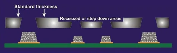
Step stencil thickness refers to the localized variations in foil depth within a single stencil, typically ranging from thinner sections for precision to thicker ones for volume. Unlike uniform stencils, step designs incorporate step-down areas etched to reduce height for fine-pitch components and step-up regions built up for high-volume needs. This approach ensures consistent solder paste volume tailored to component size, minimizing defects in high-density PCB designs. In SMT assembly, improper thickness leads to issues such as tombstoning on small chips or voiding under large pads, compromising reliability. Industry guidelines emphasize step stencils for boards with pitch variations below 0.65 mm alongside larger devices. Ultimately, selecting the right values supports efficient production and aligns with PCB design goals for miniaturization.
The relevance stems from evolving component trends toward smaller footprints, demanding thinner stencils without sacrificing paste for power devices. Step stencils enable mixed assembly without multiple printing cycles, saving time and reducing handling risks. They maintain aperture integrity across heights, crucial for maintaining area ratios during paste release. Engineers benefit from troubleshooting fewer print defects, as thickness directly influences shear and transfer efficiency. For PCB design teams, integrating step specifications early prevents costly respins.
Technical Principles Behind Stencil Thickness Selection
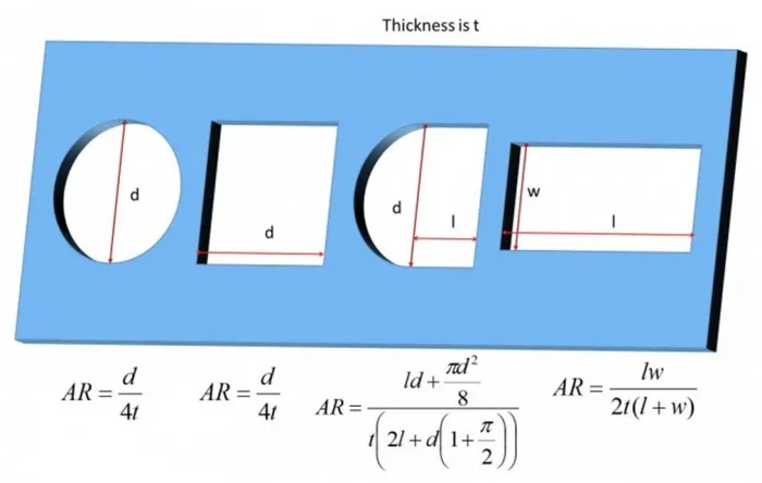
Stencil thickness primarily governs solder paste volume, calculated as aperture area multiplied by foil depth and transfer efficiency, typically 70 to 90 percent. Thinner foils, around 0.10 mm, deposit less paste ideal for components under 0.5 mm pitch, reducing bridging risks during reflow. Conversely, thicker sections up to 0.15 mm or more provide ample volume for larger component sizes, ensuring robust fillet formation. The key metric is the area ratio, defined as (aperture width plus length) divided by twice the thickness, recommended above 0.66 per IPC-7525 guidelines for reliable release.Deviations below this threshold trap paste, causing incomplete transfers.
Component size dictates minimum thickness to avoid excessive paste heights that promote shorts between adjacent pads. For fine-pitch like 0201 resistors, thicknesses below 0.10 mm enhance precision, while QFNs or BGAs with thermal pads require stepped increases. Pitch spacing influences aspect ratio, where aperture width over thickness should exceed 1.5 for clean printing. Paste rheology and printer parameters interact with thickness, as nano-scale particles demand optimized shear for homogeneity. PCB design must account for these in Gerber files, specifying steps accurately.
Surface tension during snap-off further ties thickness to release quality, with thinner foils promoting cleaner edges. Etch factors in laser-cut stencils affect wall angles, influencing paste rollback. Step height differences ideally stay under 0.05 mm to prevent uneven pressure during printing. These principles guide engineers in simulating volumes pre-production.
Factors Influencing Ideal Step Stencil Thickness
Component size emerges as the primary driver, with smaller packages like 01005 or 0201 needing 0.075 to 0.10 mm to control minute volumes precisely. Larger devices such as SOICs or power QFPs benefit from 0.125 to 0.15 mm for sufficient standoff post-reflow. Pitch below 0.4 mm mandates the thinnest steps to maintain ratios, while wider pitches allow flexibility. Solder paste volume targets derive from land patterns, often per IPC-7351 land pattern standards, ensuring joint integrity without excess.
Board layout complexity necessitates mapping thickest and thinnest zones, prioritizing the smallest component for baseline thickness. Step-up areas for through-hole pins or large BGAs add volume without compromising fine areas. Printer capabilities limit maximum steps, typically two levels per stencil. Material choices like stainless steel or nickel affect durability across varying thicknesses. Environmental factors, including humidity, influence paste behavior on different depths.
Aperture shapes, U-shaped for thermal pads, modify effective volume independent of thickness. Troubleshooting starts with SPI data, adjusting steps iteratively. These factors interplay, requiring holistic PCB design review.
Practical Best Practices for Determining Step Stencil Thickness
Start by identifying the finest pitch component to set the thinnest step, typically 0.10 mm for 0.5 mm pitch, scaling up for coarser areas. Use IPC-7525 to verify area ratios exceed 0.66 across apertures, adjusting dimensions if needed. Simulate paste volumes with software mirroring J-STD-001 joint requirements for fillet heights. Prototype with trial prints, measuring deposits via SPI for 75 to 125 percent volume targets relative to nominal.
For mixed boards, limit step heights to 0.025 to 0.05 mm differences to ensure uniform squeegee pressure. Etch thinner areas first in fabrication for precision. Validate with reflow profiles matching component specs. Document steps in assembly instructions for repeatability.
Incorporate fiducials near step transitions for alignment accuracy. Clean stencils frequently, as residue buildup varies by thickness. These practices yield high first-pass rates in SMT assembly.
Related Reading: The Impact of Stencil Thickness on Solder Joint Quality: A Detailed Analysis
Troubleshooting Common Issues with Incorrect Stencil Thickness
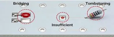
Insufficient solder paste volume on large components signals overly thin steps, leading to opens or head-in-pillow defects post-reflow. Increase thickness incrementally by 0.01 mm, rechecking ratios. Bridging on fine-pitch areas points to thick foils trapping paste; thin down while preserving volume elsewhere via aperture tweaks. Tombstoning arises from volume imbalance, resolved by stepping precisely per component size.
Poor release, evidenced by stringing, violates area ratio thresholds; recalculate per IPC-7525. Uneven prints from excessive step heights cause squeegee skipping; flatten transitions. Voids under BGAs trace to low volume on thick pads; step-up targeted areas. Analyze X-ray and AOI data to pinpoint thickness mismatches. Iterative adjustment, starting from baseline simulations, resolves most issues efficiently.
Related Reading: Mastering Step Up Stencils: A Comprehensive Guide for PCB Assembly
Case Study: Optimizing a Mixed-Component Telecom Board
Consider a telecom PCB with 0.4 mm pitch BGAs alongside large electrolytic capacitors. Initial uniform 0.125 mm stencil caused bridging on BGAs and weak joints on caps. Switching to step-down 0.10 mm for BGAs and step-up 0.15 mm for caps balanced volumes, achieving 95 percent first-pass yield. SPI confirmed ratios above 0.66, with reflow voids under 5 percent. This adjustment cut rework by half, validating thickness selection process. Lessons applied to similar high-density designs.
Conclusion
Selecting ideal step stencil thickness hinges on component size, pitch, and volume needs, guided by area ratio principles. Thinner steps ensure precision for fine features, while thicker ones secure reliability for larger parts in SMT assembly. Practical steps like simulations and trials, aligned with standards, minimize defects. PCB design teams gain from early integration, enhancing overall yields. Prioritize these factors for robust assemblies.
FAQs
Q1: What is the typical stencil thickness for fine-pitch components in PCB design?
A1: For components with pitches under 0.5 mm, such as 0201 chips or 0.4 mm BGAs, a step-down thickness of 0.075 to 0.10 mm is common. This controls solder paste volume to prevent bridging while maintaining release efficiency above 0.66 area ratio per IPC-7525. Always verify with aperture simulations tailored to your SMT assembly setup. Thicker baselines risk defects on dense boards.
Q2: How does stencil thickness affect solder paste volume in SMT assembly?
A2: Stencil thickness directly scales paste volume as area times depth times efficiency. Thinner foils reduce deposits for small component sizes, minimizing shorts; thicker ones boost volume for larger pads. Step designs optimize both on mixed PCBs. Monitor via SPI to hit 80-120 percent targets, adjusting for paste type and printer speed.
Q3: When should you use step stencils versus uniform ones for PCB design?
A3: Opt for step stencils on boards mixing fine-pitch under 0.5 mm with large components needing high volume. Uniform works for consistent sizes but fails diverse layouts, causing imbalances. Steps allow precise control per zone, improving yields. Limit height differences to 0.05 mm max for print stability.
Q4: How do you calculate the right stencil thickness for component size variations?
A4: Base on smallest pitch for the thinnest step, ensuring area ratio over 0.66. For larger component sizes, step-up to add volume without altering fine areas. Use land patterns from IPC-7351 as reference for joints. Prototype prints confirm, tweaking apertures if volumes skew.
References
IPC-7525B — Stencil Design Guidelines. IPC, 2011
IPC-7351C — Generic Requirements for Surface Mount Design and Land Pattern Standard. IPC, 2014
J-STD-001G — Requirements for Soldered Electrical and Electronic Assemblies. IPC/JEDEC, 2017


