ALLPCB


Stencil thickness plays a central role in surface mount technology assembly because it directly governs the amount of solder paste deposited on each pad. Engineers must balance this thickness to achieve reliable joints without introducing defects such as bridges or insufficient solder. Proper selection supports consistent manufacturing yields across diverse board designs. The process requires attention to component footprints, board layout density, and reflow conditions. Industry practice shows that small adjustments in thickness often produce measurable improvements in joint quality.
Why Stencil Thickness Matters in Modern PCB Assembly
Stencil thickness determines the volume of solder paste transferred through the apertures during printing. Too little paste leads to weak mechanical connections and electrical opens, while excess paste increases the risk of shorts between closely spaced leads. In high-density boards, this balance becomes especially critical because component pitches continue to shrink. Engineers therefore treat thickness as a primary control variable that influences both process capability and long-term reliability. Consistent control also reduces rework rates and supports higher first-pass yields on production lines.
Related Reading: Decoding Stencil Thickness: A Comprehensive Guide for PCB Assembly Success
Technical Principles Behind Solder Paste Volume Control
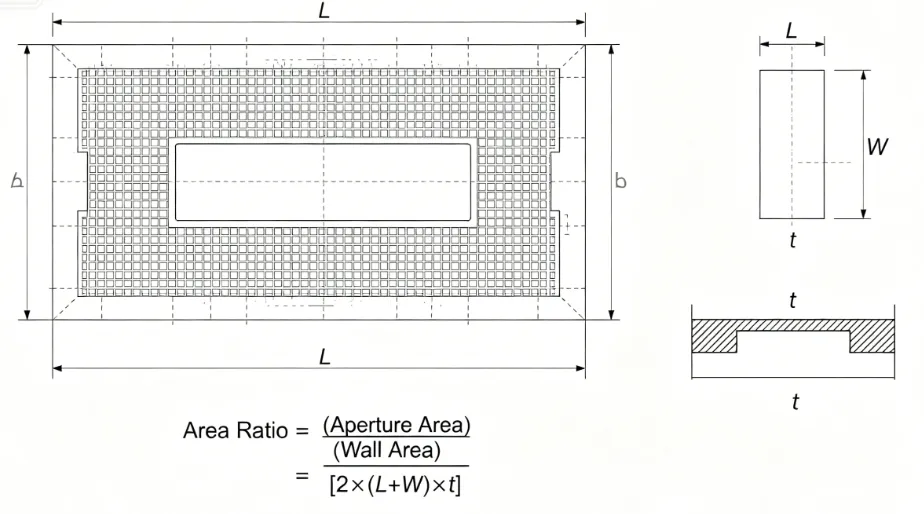
Solder paste volume is calculated from aperture area multiplied by stencil thickness, adjusted for paste transfer efficiency. The area ratio, defined as the ratio of aperture opening area to the aperture wall area, serves as the most widely accepted guideline for predicting print quality. When the area ratio falls below 0.66, paste release becomes unreliable and volume control suffers. Aspect ratio, which compares aperture width to stencil thickness, provides an additional check, with values below 1.5 often requiring process adjustments. These geometric relationships explain why a single thickness rarely suits every component on a mixed-technology board.
Stencil Thickness Guidelines for Different Components
Fine-pitch quad flat packages and ball grid arrays typically require thinner stencils to maintain acceptable area ratios on small pads. In contrast, larger passive components such as 1206 resistors tolerate thicker stencils that deliver greater paste volume for improved fillet formation. Engineers often segment the stencil into zones, applying different thicknesses or stepped reliefs where component sizes vary widely. This zoned approach preserves volume control without forcing a compromise thickness across the entire board. Practical experience confirms that matching thickness to the most demanding footprints first, then verifying the remainder, yields the most stable printing process.
Stencil Thickness Calculation Methods and Area Ratio Considerations
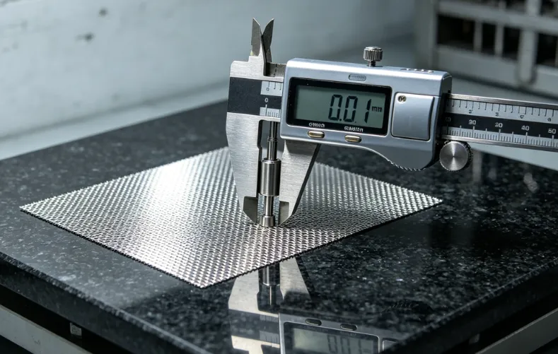
Calculation begins with the target solder paste volume required for each joint, derived from pad geometry and desired fillet height. Once volume is established, thickness is solved by dividing volume by aperture area, after which the resulting area ratio is checked against recommended limits. When the ratio falls short, aperture modifications or local thickness changes become necessary. Engineers document these calculations in the stencil design package so that manufacturing teams can reproduce the same volume targets on subsequent builds. This structured method reduces trial-and-error iterations during new product introduction.
Related Reading: Step Stencil Thickness: How to Determine the Ideal Value for Your PCB
Practical Best Practices for Maintaining Optimal Volume
Process engineers verify stencil thickness at incoming inspection using calibrated micrometers or laser gauges to confirm conformance with the design specification. During production, regular cleaning cycles prevent paste buildup that can alter effective thickness and degrade volume consistency. When print quality drifts, thickness is rechecked before other variables such as squeegee pressure or speed are adjusted. Documentation of thickness values alongside measured paste volumes creates a traceable record that supports continuous improvement efforts. These steps align with established quality practices outlined in IPC standards for stencil design and use.
Troubleshooting Common Volume-Related Issues
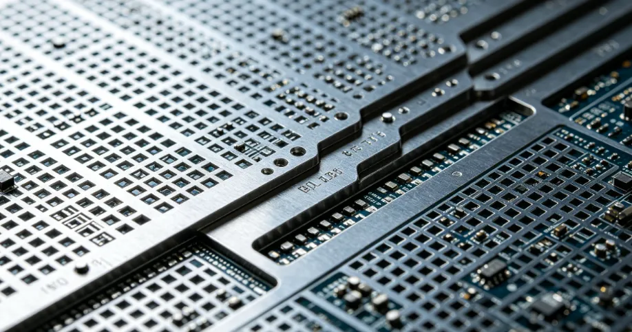
Insufficient paste volume on small pads often traces back to an area ratio below the recommended threshold, prompting either aperture enlargement or a local reduction in stencil thickness. Excessive volume on fine-pitch leads frequently results from an overly thick stencil that exceeds the aspect ratio limit, leading to bridging after reflow. In both cases, systematic measurement of printed paste height with laser scanners provides quantitative data to guide corrective thickness changes. Engineers record these adjustments and revalidate the process before releasing the revised stencil for volume production. This methodical troubleshooting approach minimizes downtime and preserves yield targets.
Conclusion
Selecting the appropriate stencil thickness requires careful consideration of area ratio, component mix, and target paste volume. Logical application of these principles enables engineers to achieve repeatable solder joints across a wide range of board designs. Regular verification and documentation further ensure that the chosen thickness remains effective throughout the product lifecycle. By focusing on these engineering fundamentals, manufacturing teams can improve both quality and efficiency without unnecessary complexity.
FAQs
Q1: What factors influence stencil thickness calculation for reliable solder paste volume?
A1: Stencil thickness calculation begins with the required paste volume for each joint, followed by verification of the area ratio and aspect ratio. Engineers adjust thickness to keep these ratios within accepted limits while accommodating the full range of component sizes on the board. This structured approach ensures consistent deposition across production runs.
Q2: How does stencil thickness affect solder paste volume control during printing?
A2: Stencil thickness directly multiplies the aperture area to determine the theoretical paste volume transferred to each pad. Deviations from the calculated thickness alter actual deposited volume, which can cause opens or bridges after reflow. Maintaining tight control over thickness therefore forms the foundation of stable volume control.
Q3: What stencil thickness guidelines apply to different components on the same PCB?
A3: Guidelines recommend thinner sections for fine-pitch devices to preserve acceptable area ratios, while thicker sections suit larger passives that need greater volume. Zoned or stepped stencil designs allow these differing requirements to coexist on a single foil. Engineers validate the final configuration through test prints before committing to production.
Q4: Why is the area ratio important when selecting stencil thickness?
A4: The area ratio predicts how cleanly paste releases from the aperture walls, with lower values indicating higher risk of incomplete transfer. Selecting thickness that keeps the ratio above established thresholds helps maintain the intended solder paste volume. This relationship guides most practical stencil thickness decisions in modern assembly.
References
IPC-7525B — Stencil Design Guidelines. IPC, 2018
J-STD-001H — Requirements for Soldered Electrical and Electronic Assemblies. IPC, 2020
IPC-A-610G — Acceptability of Electronic Assemblies. IPC, 2017