 ALLPCB


What Are SMD and NSMD Pads and Why the Distinction Matters
Solder mask defined pads and non-solder mask defined pads represent two fundamental approaches to defining the solderable area on a printed circuit board. Engineers select between these PCB pad types based on component pitch, assembly process requirements, and long-term reliability targets. Fine pitch components such as ball grid arrays and quad flat no-lead packages place particular emphasis on precise control of solder joint geometry. The choice between SMD pads and NSMD pads influences solder volume, stress distribution during thermal cycling, and susceptibility to manufacturing defects. Understanding the mechanical and process implications helps designers optimize layouts for both prototype and volume production.
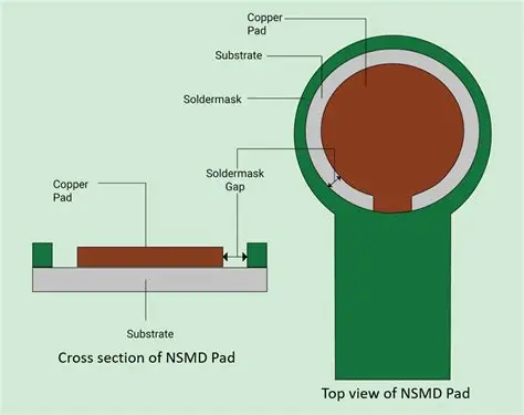
SMD pads feature a solder mask opening smaller than the underlying copper pad, so the mask aperture determines the final solderable surface. NSMD pads reverse this relationship, with the copper pad smaller than the solder mask opening, allowing the copper edge to define the boundary. The distinction affects how much copper remains exposed and how solder wets during reflow. In high-density designs, this choice directly influences the risk of solder bridging between adjacent pads. Proper selection also supports consistent stencil aperture design and paste release characteristics across a panel.
Industry standards such as IPC-A-600 provide acceptance criteria that apply equally to both configurations when evaluating finished boards. The decision becomes especially relevant when component leads or balls approach 0.5 mm pitch or below, where small variations in pad definition can shift from acceptable to marginal yields.
Technical Principles of Solder Mask Pad Design
The solder mask layer serves as a dielectric barrier that prevents unintended solder flow while protecting underlying copper from oxidation and environmental exposure. In an SMD configuration the mask overlaps the copper pad edges, reducing the effective pad diameter and concentrating solder volume within a smaller footprint. This overlap can increase the height of the resulting solder joint for a given paste deposit. NSMD designs leave a clearance between the copper edge and the mask opening, permitting solder to wet the full copper perimeter and form a fillet that distributes mechanical stress more evenly.
Thermal expansion mismatch between the component package and the board generates cyclic shear forces at the solder joint. The geometry created by each pad type alters the stress concentration points. SMD pads tend to produce a more cylindrical joint shape, while NSMD pads allow a slightly larger contact area at the board interface. Both configurations must satisfy the dimensional tolerances outlined in relevant IPC specifications for land pattern accuracy and mask registration.
Practical Design and Manufacturing Considerations
Designers typically begin by reviewing the component datasheet land pattern recommendations and then adjust for the chosen pad definition. For fine pitch components, NSMD pads often provide improved solder joint reliability under thermal cycling because the copper-to-solder interface experiences lower stress concentration. SMD pads can simplify mask design rules on very dense layouts by allowing tighter mask-to-mask spacing without risking copper exposure. Stencil design must account for the final exposed area rather than the nominal copper size to maintain consistent paste volume.
Registration tolerances between the solder mask and copper layers become critical. Excessive mask encroachment on an SMD pad can reduce the solderable area below acceptable limits, while insufficient clearance on an NSMD pad may allow solder to wet unintended copper. Fabrication notes should specify mask expansion values and minimum annular ring requirements consistent with the selected pad type. Assembly teams benefit from clear documentation of which pads follow each definition so that inspection criteria can be applied correctly.
Best Practices for Selecting Pad Types
Evaluate the component pitch first. Pitches below 0.65 mm frequently favor NSMD pads to maximize solder joint robustness. Larger pitch components may use SMD pads when board real estate is constrained or when mask-defined openings simplify routing. Consider the expected thermal profile and end-use environment. Applications involving repeated temperature excursions benefit from the stress distribution advantages of NSMD geometry. Review the entire bill of materials to ensure stencil apertures remain compatible across all pad types on the same assembly.
Coordinate with the fabrication and assembly partners early in the layout phase. Provide explicit layer-specific notes indicating mask expansion or contraction values for each pad group. Verify that the chosen definition aligns with the board shop’s minimum mask feature size and registration capability. When mixing both pad types on a single board, maintain consistent mask-to-copper clearance rules to avoid process variation.
Conclusion
SMD pads and NSMD pads each offer distinct advantages depending on component pitch, reliability requirements, and manufacturing constraints. NSMD configurations generally improve solder joint durability for fine pitch components, while SMD pads can simplify mask layout in space-limited areas. The final selection should follow a structured review of land pattern recommendations, thermal expectations, and process capabilities. Consistent application of these principles across a design reduces both assembly defects and field failures.
FAQs
Q1: What is the primary difference between SMD pads and NSMD pads in solder mask pad design?
A1: SMD pads use the solder mask opening to define the solderable area, while NSMD pads allow the copper pad itself to define that area. The choice affects solder volume, joint shape, and stress distribution. Engineers evaluate both options against component pitch and reliability targets.
Q2: When should designers prefer NSMD pads for fine pitch components?
A2: NSMD pads are often selected for fine pitch components because they permit a larger copper-to-solder interface that distributes thermal stress more effectively. This configuration supports improved joint reliability under temperature cycling. Layout teams confirm the approach against land pattern guidelines and fabrication tolerances.
Q3: How does solder mask registration tolerance affect SMD versus NSMD pad performance?
A3: Registration errors on SMD pads can reduce the effective solderable area, while the same error on NSMD pads may allow unintended copper exposure. Both situations influence paste volume consistency and final joint geometry. Clear fabrication notes help maintain acceptable registration across production panels.
Q4: Can SMD and NSMD pads be mixed on the same PCB?
A4: Yes, many designs combine both pad types when component requirements differ across the board. Consistent mask expansion rules and clear documentation ensure the assembly process remains repeatable. Early coordination with manufacturing partners confirms compatibility with stencil and inspection processes.
References
IPC-A-600K — Acceptability of Printed Boards. IPC, 2020
IPC-6012E — Qualification and Performance Specification for Rigid Printed Boards. IPC, 2017
IPC-SM-840E — Qualification and Performance Specification of Permanent Solder Mask and Flexible Cover Materials. IPC, 2010


