 ALLPCB


Why Solar Inverter PCB Assembly Matters
Solar inverters operate continuously under varying loads, temperature swings, and humidity levels. The PCB assembly must handle high currents while maintaining signal integrity for control circuits. Manufacturers therefore prioritize robust assembly processes that meet both electrical and mechanical requirements. Consistent quality in solar inverter PCB assembly reduces field failures and supports warranty commitments across large installations.
Core Technical Principles
Solar inverter PCBs typically combine surface-mount technology with through-hole components. Power semiconductors, inductors, and capacitors often require through-hole mounting for mechanical strength and heat dissipation. Control and sensing circuits rely on SMT assembly for higher component density and automated placement accuracy. Thermal management becomes critical because power losses generate localized heat that can degrade solder joints over time.
Industry standards guide acceptable workmanship levels. IPC-A-610 defines visual acceptance criteria for electronic assemblies, including solder joint appearance and component placement tolerances. Manufacturers apply these criteria during inspection to ensure assemblies withstand vibration and thermal cycling typical of solar installations.
Step-by-Step Assembly Process
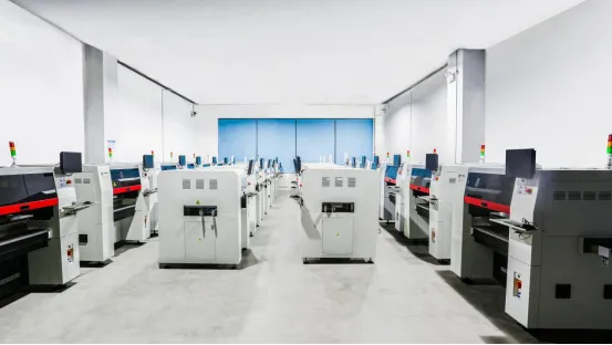
The process begins with incoming PCB inspection for warpage, cleanliness, and pad integrity. Stencils apply solder paste to surface-mount pads with controlled volume and alignment. Automated placement machines position components according to the bill of materials and coordinate data. Reflow soldering follows in a controlled thermal profile that activates flux, melts solder, and forms reliable joints without damaging temperature-sensitive parts.
Through-hole components are inserted next, either manually or with automated insertion equipment. Wave soldering or selective soldering attaches these larger parts while protecting previously soldered SMT components. Hand soldering addresses any remaining connections or rework requirements using temperature-controlled tools and appropriate flux.
After soldering, assemblies undergo cleaning to remove flux residues that could cause corrosion or leakage currents. Conformal coating may then be applied in areas exposed to moisture. Final steps include in-circuit testing, functional verification under simulated load conditions, and burn-in to identify early failures.
Quality Control and Best Practices
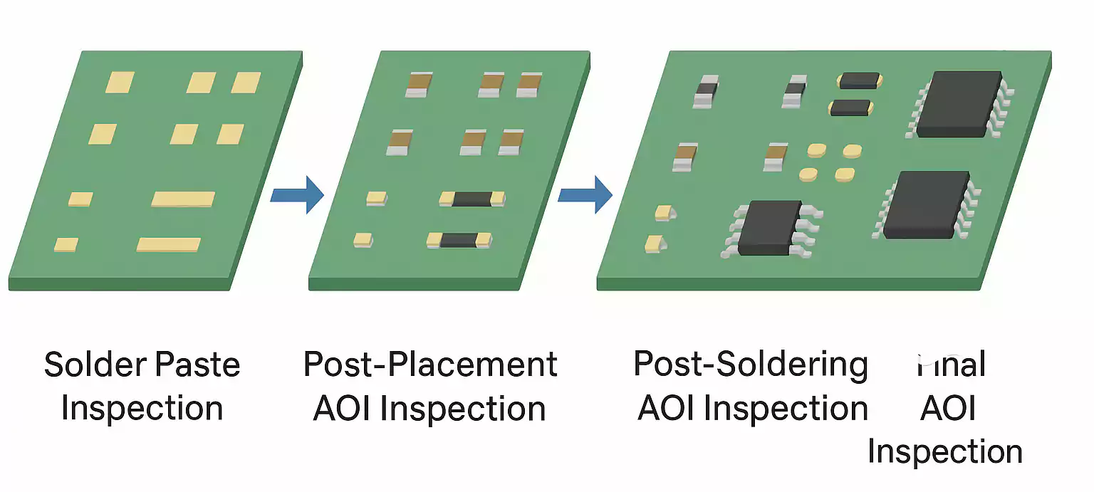
Visual inspection, automated optical inspection, and X-ray imaging verify solder joint quality, especially for bottom-terminated components such as QFNs and BGAs common in inverter control sections. Electrical testing confirms continuity, isolation, and parametric performance. Thermal imaging during functional test identifies hot spots that could indicate poor thermal interface or component issues.
Manufacturers follow J-STD-001 for soldering process requirements, covering material selection, equipment calibration, and operator training. Process control records track temperature profiles, paste viscosity, and placement accuracy to maintain repeatability across production batches.
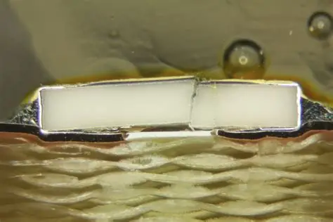
Troubleshooting often centers on solder defects such as bridges, insufficient wetting, or head-in-pillow phenomena in larger packages. Root-cause analysis examines stencil design, reflow atmosphere, component coplanarity, and PCB surface finish. Adjustments to flux activity or peak temperature typically resolve most issues when performed systematically.
Practical Considerations for Manufacturers
Design for manufacturability reviews should occur early, addressing component spacing, thermal relief patterns, and test point accessibility. Panelization strategies balance throughput with handling stresses that could induce warpage. Material selection favors laminates with appropriate glass transition temperatures and coefficients of thermal expansion matched to expected operating conditions.
Documentation of every process parameter supports traceability and continuous improvement. Statistical process control monitors key metrics such as solder paste volume and placement accuracy, enabling early detection of drift before defects reach later stages.
Conclusion
Effective solar inverter PCB assembly integrates SMT assembly, through-hole assembly, and controlled PCB soldering techniques within a disciplined manufacturing process. Attention to thermal profiles, inspection criteria, and process documentation yields assemblies that meet the reliability demands of photovoltaic systems. Manufacturers who align their operations with established industry standards consistently achieve higher first-pass yields and lower warranty costs.
FAQs
Q1: What distinguishes solar inverter PCB assembly from standard electronics assembly?
A1: Solar inverter PCB assembly combines high-current through-hole components with dense SMT circuitry while emphasizing thermal management and long-term reliability under outdoor conditions. The process incorporates stricter inspection and testing protocols to handle continuous operation and environmental stress.
Q2: How do SMT assembly and through-hole assembly work together in solar inverters?
A2: SMT assembly places smaller control and sensing components for density and automation, while through-hole assembly secures power devices that require mechanical strength and heat sinking. Sequential processing ensures previously soldered areas remain protected during later high-temperature steps.
Q3: Which PCB soldering techniques are most common for solar inverter boards?
A3: Reflow soldering dominates SMT joints, wave or selective soldering attaches through-hole parts, and limited hand soldering addresses exceptions or repairs. Each technique follows controlled thermal profiles to achieve consistent intermetallic formation without component damage.
Q4: Why is process control important in PCB manufacturing process for inverters?
A4: Process control maintains consistent solder joint quality, placement accuracy, and cleanliness across batches, directly affecting inverter efficiency and field longevity. Documented parameters allow rapid identification and correction of deviations before they impact finished assemblies.
References
IPC-A-610H — Acceptability of Electronic Assemblies. IPC, 2020
J-STD-001H — Requirements for Soldered Electrical and Electronic Assemblies. IPC, 2020
IPC-6012E — Qualification and Performance Specification for Rigid Printed Boards. IPC, 2017





