 ALLPCB


Introduction
In modern electronics design, PCB footprint simulation plays a critical role in ensuring that component landing patterns perform reliably under real-world conditions. Electrical engineers often face challenges where small discrepancies in pad geometry or spacing lead to signal degradation, overheating, or assembly failures after production. By conducting PCB footprint simulation early, teams can validate designs through signal integrity analysis, thermal simulation, and overall PCB design validation, reducing iteration costs and time-to-market. This approach aligns with industry needs for high-density boards in applications like telecommunications and automotive systems. Ultimately, simulation bridges the gap between design intent and manufacturing outcomes, fostering robust performance.
What Is PCB Footprint Simulation and Why It Matters
PCB footprint simulation refers to the computational modeling of component land patterns on a printed circuit board to predict electrical, thermal, and mechanical behaviors before fabrication. These footprints, which include pads, vias, and silkscreen elements, must accommodate precise component placement while minimizing risks like solder joint voids or trace impedance mismatches. Signal integrity analysis within this process evaluates how footprints affect high-speed signal propagation, while thermal simulation assesses heat dissipation from power components. For electrical engineers, this validation is essential because production errors can cascade into field failures, increasing warranty costs and damaging reliability reputations.
The relevance of PCB footprint simulation grows with shrinking node sizes and multilayer boards, where tolerances are tighter. Poorly designed footprints can cause crosstalk in adjacent traces or insufficient thermal relief, leading to hotspots that exceed material limits. Industry data underscores that early PCB design validation through simulation catches up to 80 percent of potential issues, preventing expensive respins. Moreover, compliance with established guidelines ensures interoperability across supply chains. In high-reliability sectors, neglecting this step compromises system longevity and performance metrics.
Core Technical Principles of PCB Footprint Simulation
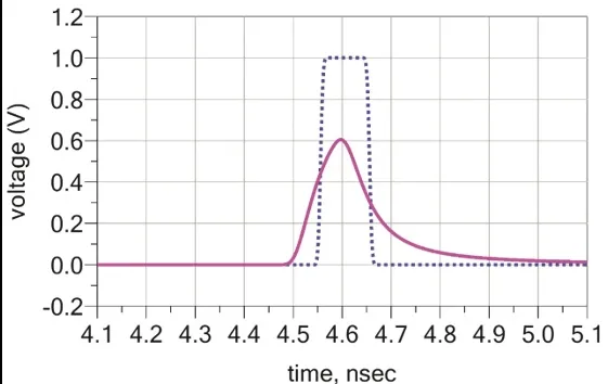
At its foundation, PCB footprint simulation relies on finite element analysis and electromagnetic field solvers to model interactions at the pad level. For signal integrity analysis, simulations compute characteristic impedance based on pad width, spacing, and dielectric properties surrounding the footprint. Variations in land pattern geometry directly influence return path integrity and insertion loss, particularly for differential pairs. Engineers must account for via transitions within footprints, as stub effects can degrade eye diagrams at gigabit speeds. These principles ensure that simulated waveforms match expected margins before committing to fabrication.
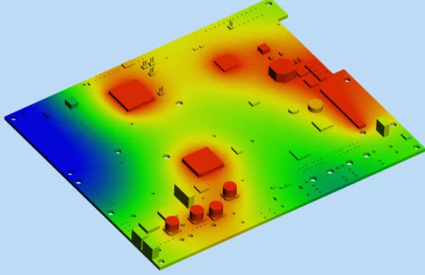
Thermal simulation in PCB footprints focuses on conduction, convection, and radiation from component junctions through pads and planes. Heat spreading occurs via copper pours and thermal vias integrated into the footprint design, with simulations revealing gradient distributions across layers. Material thermal conductivity and thickness play key roles, as do boundary conditions mimicking ambient airflow. Overlooking these can result in junction temperatures surpassing safe thresholds, accelerating electromigration. Structured modeling allows quantification of theta-JA values for validation against operational envelopes.
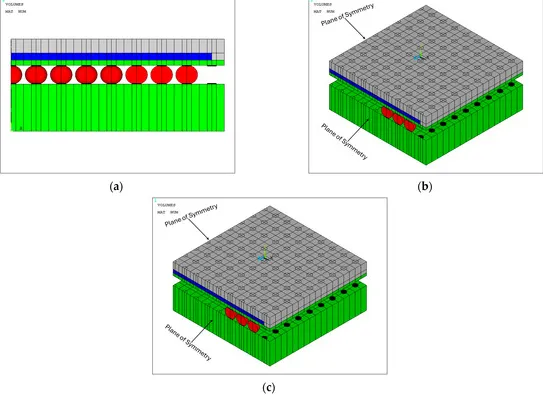
Mechanical aspects involve solder joint simulation, predicting stress from coefficient of thermal expansion mismatches between components and boards. Finite element models apply cyclic loading to forecast fatigue life in footprints with fine-pitch arrays. Pad overhang and fillet formation influence joint strength, guiding geometry optimizations. This holistic approach in PCB design validation integrates all domains for comprehensive predictions.
Signal Integrity Analysis in PCB Footprints
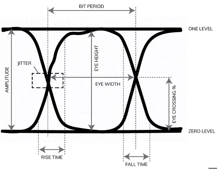
Signal integrity analysis begins with extracting S-parameters from footprint models to identify reflections and crosstalk. Pad-to-pad coupling depends on edge-to-edge distances, with simulations optimizing courtyard boundaries to maintain isolation. For high-speed interfaces, footprint symmetry ensures balanced propagation delays, critical for clock distribution networks. Engineers iterate geometries to achieve target impedance, typically 50 or 100 ohms, while minimizing via resonances. Pre-layout checks via 2D field solvers provide quick feedback, transitioning to full 3D for complex BGA footprints.
Crosstalk mitigation involves shielding and ground plane proximity within the footprint vicinity. Simulations quantify near-end and far-end coupling voltages under worst-case aggressor switching. Compliance with routing rules extends to footprint selection, ensuring via-in-pad configurations support dense layouts without performance penalties. This targeted analysis prevents bit error rates from escalating in production prototypes.
Thermal Simulation Techniques for Footprints
Thermal simulation employs computational fluid dynamics coupled with conduction models to map isotherms across footprints. Power dissipation from ICs flows through thermal pads, necessitating via arrays for interlayer heat transfer. Simulations incorporate board stackup, revealing how plane cuts affect spreading angles. Engineers evaluate multiple scenarios, from natural convection to forced air, to establish safe operating windows. Adherence to guidelines like IPC-2152 for current-carrying capacity informs trace widths adjacent to footprints.
Hotspot prediction guides via placement density and copper balancing within the footprint. Transient analyses capture peak temperatures during power-up transients, vital for power management ICs. Material selection, such as high-Tg laminates, further refines models for accuracy. These techniques enable proactive PCB design validation, avoiding delamination risks in reflow profiles.
Mechanical and Assembly Validation
Mechanical simulation assesses warpage induced by footprint asymmetry under thermal loads. Bow and twist calculations use bilayer models, predicting standoff heights for reliable soldering. Solder volume modeling per land pattern standards ensures fillet formation without bridging. Drop and vibration tests simulate joint shear stresses, prioritizing robust toe and heel geometries. This validation extends to fiducials for pick-and-place accuracy.
Best Practices for Effective PCB Footprint Simulation
Start with standardized land patterns as outlined in IPC-7351 to establish baseline geometries for simulation inputs. Collaborate across disciplines, integrating mechanical CAD data for precise component models. Employ parametric sweeps to explore tolerances, focusing on yield impacts from pad shrinkage. Verify simulations against empirical data from test coupons, refining mesh densities for convergence. Document assumptions, including material libraries and boundary conditions, for reproducibility.
Layer stackup optimization complements footprint simulation, with power and ground planes enhancing both SI and thermal performance. Incorporate guard traces around sensitive footprints to suppress EMI. For high-power designs, simulate under overcurrent conditions to stress-test joints. Regular design reviews ensure simulations align with fabrication capabilities. These practices solidify PCB design validation workflows.
Incorporate design for manufacturing by simulating stencil apertures relative to pad sizes. This predicts solder paste release and reflow outcomes, minimizing defects like head-in-pillow. Cross-check with IPC-2221 principles for overall board integrity. Iterative refinement based on sensitivity analyses yields resilient designs.
Common Challenges and Solutions in Simulation
One challenge arises from model fidelity, where simplified 2D approximations overlook 3D effects in dense footprints. Transition to hybrid solvers balances accuracy and compute time. Variability in component lead coplanarity requires Monte Carlo simulations for statistical reliability. Address this by defining guardbands in pad sizing.
Thermal crosstalk between adjacent footprints demands zoned airflow modeling. Solutions include dedicated heat sinks or moats, validated through coupled electro-thermal sims. For signal integrity, parasitic extraction post-layout confirms footprint contributions to total channel loss. Troubleshooting focuses on root-cause isolation via decomposition.
Conclusion
PCB footprint simulation stands as a cornerstone of modern PCB design validation, integrating signal integrity analysis, thermal simulation, and mechanical checks for production-ready outcomes. Electrical engineers benefit from reduced risks, faster iterations, and enhanced performance in complex systems. Adopting structured workflows with industry-aligned practices ensures footprints support demanding applications. Ultimately, this proactive validation elevates design quality, reliability, and cost efficiency across the product lifecycle.
FAQs
Q1: What role does PCB footprint simulation play in signal integrity analysis?
A1: PCB footprint simulation is essential for signal integrity analysis as it models pad geometries to predict impedance mismatches and crosstalk in high-speed signals. Engineers simulate trace transitions and via stubs to ensure clean eye patterns and low insertion loss. This early validation prevents production failures by optimizing courtyard spacing and symmetry. Compliance with design guidelines further refines outcomes for gigabit interfaces.
Q2: How does thermal simulation validate PCB footprints?
A2: Thermal simulation in PCB footprints quantifies heat flow from components through pads and vias, identifying hotspots before production. It accounts for stackup, copper planes, and convection to compute junction temperatures under load. Engineers use this for via farm sizing and plane cutouts, ensuring dissipation meets requirements. This process supports reliable operation in power-dense designs.
Q3: Why is IPC footprint simulation important for PCB design validation?
A3: IPC footprint simulation standardizes land patterns for optimal solderability and performance, crucial for PCB design validation. It guides pad dimensions across density levels, reducing assembly defects. Simulations based on these ensure mechanical robustness and electrical integrity. Electrical engineers rely on this for consistent, manufacturable designs across projects.
Q4: What are best practices for PCB footprint simulation workflows?
A4: Best practices include starting with verified component models, performing multi-physics simulations, and iterating based on sensitivity studies. Integrate signal integrity analysis and thermal checks early, documenting all parameters. Validate against test data and collaborate with fabrication teams. This structured approach minimizes respins and enhances overall PCB reliability.
References
IPC-7351B — Generic Requirements for Surface Mount Design and Land Pattern Standard. IPC, 2005
IPC-2152 — Standard for Determining Current Carrying Capacity in Printed Board Trace. IPC, 2009
IPC-2221C — Generic Standard on Printed Board Design. IPC, 2023


