 ALLPCB


Multilayer Magic: How Total PCB Thickness Affects Routing Density and Signal Integrity
Introduction
Multilayer printed circuit boards enable complex electronic designs by stacking multiple conductive layers separated by insulating materials. Total PCB thickness plays a central role in determining how densely traces can be routed and how well signals maintain integrity across those layers. Engineers often evaluate thickness early in the design cycle because it influences both manufacturability and electrical performance. Selecting an appropriate overall thickness requires balancing mechanical stability with the demands of high-speed signaling and fine-pitch components. This relationship becomes especially important in applications that combine dense interconnects with strict timing or impedance requirements.
What Is Multilayer PCB Thickness and Why It Matters
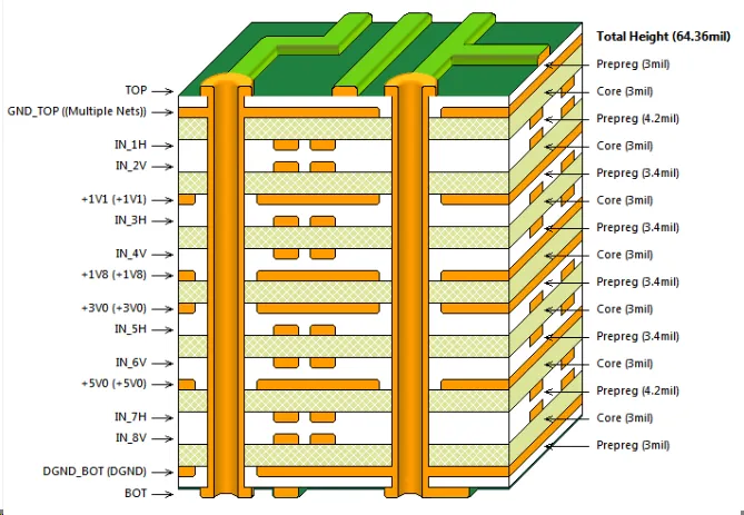
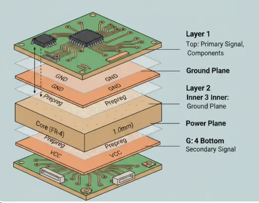
Multilayer PCB thickness refers to the finished dimension measured from the outer surface of one copper layer to the outer surface of the opposite outer layer, including all core materials, prepregs, and copper foils. This dimension directly affects the available space for routing traces between layers and the electrical characteristics of those traces. In multilayer constructions, thickness also influences thermal expansion behavior and mechanical rigidity during assembly and operation. Industry specifications such as IPC-6012E establish qualification requirements that tie finished thickness to acceptable performance levels for rigid boards. Designers therefore treat total thickness as a fundamental stackup parameter rather than a secondary detail.
How Thickness Influences Routing Density
Thicker boards provide greater separation between signal layers, which can reduce unwanted coupling but also lengthens the vertical distance that vias must traverse. This increased via length often requires larger annular rings or additional clearance, limiting the number of traces that can pass between pads in a given area. Conversely, thinner constructions allow shorter vias and tighter layer-to-layer registration, supporting higher routing density in the same footprint. The choice of core thickness and prepreg count further modulates how many signal layers can be accommodated without exceeding the target overall dimension. Engineers typically model these trade-offs during stackup planning to achieve the required interconnect density while remaining within fabrication limits.
Impact of PCB Thickness on Signal Integrity in Multilayer Designs
Signal integrity depends on controlled impedance, minimized crosstalk, and reduced propagation delay variations, all of which are sensitive to the dielectric thickness between layers. When total board thickness increases, the distance between a signal trace and its reference plane may also increase unless the stackup is adjusted accordingly. Greater separation can raise characteristic impedance or alter return-path inductance, potentially degrading rise times and increasing susceptibility to noise. Thinner profiles, when properly implemented, allow tighter coupling to reference planes and shorter via stubs, improving high-frequency performance. These effects become pronounced in designs operating above several hundred megahertz, where even small changes in dielectric spacing produce measurable differences in eye diagrams and bit-error rates.
Best Practices for PCB Stackup and Thickness Selection
Effective stackup design begins with defining target impedance values and routing density goals before selecting core and prepreg thicknesses. Symmetric constructions around the center of the board help control warpage and maintain consistent dielectric spacing across the panel. Placing critical high-speed signals on layers adjacent to solid reference planes reduces loop inductance and improves return paths. Designers also consider the cumulative effect of copper thickness on overall dimension, because plating build-up on outer layers contributes to the finished thickness. Collaboration between design and fabrication teams ensures that the chosen stackup remains compatible with standard lamination processes and meets acceptance criteria outlined in relevant industry specifications.
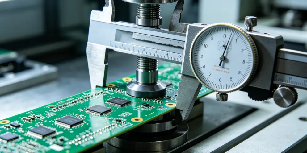
Practical Considerations During Manufacturing and Assembly
During fabrication, total thickness must remain within tolerances that allow reliable drilling, plating, and solder-mask application. Excessive variation can lead to registration issues between layers or difficulties achieving uniform via fill. In assembly, thicker boards may require adjusted reflow profiles to accommodate greater thermal mass, while thinner boards demand careful handling to avoid flexure that could damage fine features. Quality-control procedures, including those described in IPC-A-600K, verify that finished thickness and layer alignment meet the requirements established during design. These steps help ensure that the electrical benefits designed into the stackup are realized in the delivered product.
Conclusion
Total PCB thickness serves as a pivotal parameter that links routing density, signal integrity, and manufacturability in multilayer constructions. Thoughtful selection of core, prepreg, and copper thicknesses allows designers to optimize interconnect density while preserving the electrical characteristics needed for reliable high-speed operation. Adherence to established industry specifications provides a consistent framework for verifying that finished boards meet both mechanical and electrical expectations. By treating thickness as an integral part of stackup planning rather than an afterthought, engineering teams can achieve compact, high-performance layouts that perform consistently across production volumes.
FAQs
Q1: How does multilayer PCB thickness influence routing density?
A1: Greater overall thickness increases via length and clearance requirements, which can reduce the number of traces that fit between component pads. Thinner profiles shorten vertical interconnects and improve layer-to-layer registration, enabling higher routing density within the same board area. Stackup symmetry and careful selection of core thicknesses help maintain density targets without compromising manufacturability.
Q2: What role does PCB thickness play in multilayer signal integrity?
A2: Thickness affects the dielectric spacing between signal traces and reference planes, directly influencing impedance, crosstalk, and propagation characteristics. Controlled thinner constructions often provide tighter coupling and shorter via stubs that preserve signal quality at higher frequencies. Proper stackup planning ensures that thickness supports the required electrical performance rather than degrading it.
Q3: Why is PCB stackup important when specifying total board thickness?
A3: The stackup determines how individual layer thicknesses combine to reach the target overall dimension while satisfying impedance and routing needs. Symmetric arrangements around the board center reduce warpage and maintain consistent spacing. Early definition of stackup parameters prevents later conflicts between density goals and fabrication capabilities.
Q4: How do industry standards guide multilayer PCB thickness decisions?
A4: Standards such as IPC-6012E define qualification and performance requirements that include finished thickness tolerances for rigid boards. IPC-A-600K provides visual and dimensional acceptance criteria that help verify compliance after fabrication. These documents give designers and manufacturers a common reference for ensuring that thickness supports both mechanical reliability and electrical function.
References
IPC-6012E: Qualification and Performance Specification for Rigid Printed Boards.
IPC-A-600K: Acceptability of Printed Boards.


