 ALLPCB


Introduction
In high-density interconnect (HDI) printed circuit boards, microvias play a critical role in achieving compact designs with superior routing density. These small vias connect adjacent layers, enabling efficient signal and power distribution in devices like smartphones, wearables, and medical electronics. However, their minuscule dimensions limit the microvia current carrying capacity, making precise management essential to prevent overheating and reliability failures. Electrical engineers must balance miniaturization demands with thermal constraints to ensure safe power delivery. This article explores the principles of microvia ampacity, factors influencing it, and strategies for optimization aligned with industry standards.
Understanding Microvia Current Carrying Capacity and Its Importance
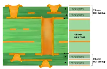
Microvias are blind or buried vias with a maximum aspect ratio of 1:1 and a total depth not exceeding 0.25 mm, distinguishing them from standard through-holes. Microvia current carrying capacity, often termed ampacity, refers to the maximum continuous current a microvia can handle without exceeding allowable temperature rise. This parameter directly impacts power delivery integrity, as insufficient capacity leads to resistive heating, electromigration, and potential delamination in the via structure. In dense HDI boards, power nets routed through microvias demand careful evaluation to avoid hotspots that degrade overall board performance.
The relevance escalates in applications requiring high-speed data and moderate power, where microvias bridge outer layers to inner power planes. Exceeding ampacity causes localized thermal stress, accelerating barrel cracking or pad cratering under thermal cycling. Engineers prioritize this during design to comply with reliability requirements, ensuring long-term operation in harsh environments. Proper assessment supports efficient power delivery, minimizing voltage drops and enhancing system efficiency.
Technical Principles Governing Microvia Ampacity
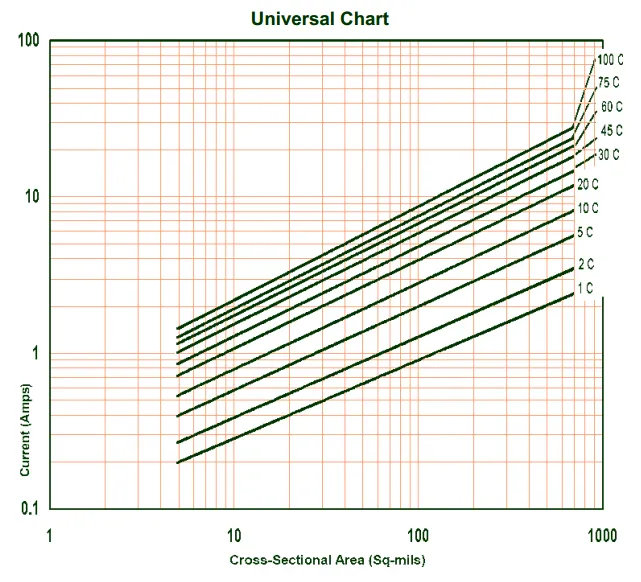
Microvia ampacity derives from the interplay of electrical resistance, thermal dissipation, and material properties. The primary conductor is the electroplated copper barrel, typically 15 to 25 microns thick, whose cross-sectional area dictates resistance via Ohm's law. Heat generation follows Joule heating, I^2R, where current density must stay below thresholds to limit temperature rise, often targeted at 10 to 20°C above ambient. IPC-2152 provides foundational charts and nomographs for conductor current capacity, adaptable to vias by considering plating geometry and board stackup.
Key factors include via diameter, plating thickness, and dielectric thickness, as smaller features concentrate current density. Aspect ratio affects plating uniformity; exceeding 0.8:1 risks voiding, reducing effective conductive area. Board-level thermal management influences dissipation, with proximity to copper planes aiding heat spreading while air gaps hinder it. In stacked microvias, series resistance compounds, necessitating derating for cumulative effects.
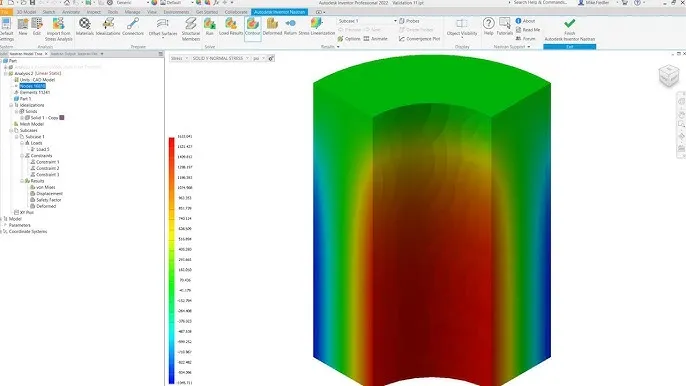
Thermal resistance models treat the via as a cylindrical resistor embedded in a composite medium. External factors like copper weight, layer count, and airflow modify the allowable current. For internal microvias, reduced surface exposure lowers ampacity compared to outer-layer ones. Simulations incorporating these variables yield precise predictions, bridging empirical data from standards to specific designs.
Microvia Power Delivery Challenges and Thermal Management
Power delivery through microvias introduces unique challenges due to their role in decoupling capacitors and plane transitions. High-frequency components demand low-impedance paths, yet microvia inductance and resistance can introduce noise if ampacity is marginal. Thermal management becomes paramount, as clustered microvias form hotspots impeding heat flow through thin dielectrics. Strategies involve balancing via farms with trace routing to distribute current evenly.
In HDI structures, microvia thermal management requires evaluating stackup symmetry and filler materials for enhanced conductivity. Unfilled microvias offer lower capacitance but poorer thermal paths; filled ones improve dissipation at the cost of process complexity. IPC-2226 outlines design rules for HDI, including microvia placement to mitigate thermomechanical stress. Engineers model power nets holistically, accounting for transient currents during switching.
Dynamic effects like skin effect at high frequencies further limit effective ampacity, prompting wider annular rings or staggered configurations. Board warpage from asymmetric heating exacerbates via reliability, underscoring integrated thermal analysis.
Best Practices for Optimizing Microvia Ampacity
Designers start by selecting via dimensions compliant with fabrication capabilities, targeting diameters from 75 to 150 microns for optimal plating. Parallel microvias multiply capacity linearly, ideal for power pins exceeding single-via limits; a farm of four doubles effective ampacity while spreading heat. Simulate using IPC-2152-derived calculators, inputting plating thickness, delta T, and environmental factors for conservative sizing.
Incorporate thermal reliefs or stitched vias adjacent to power microvias to enhance dissipation to planes. Prefer staggered stacking over stacked to reduce drill depth and improve reliability. During layout, route high-current nets preferentially on thicker copper layers, reserving microvias for signals or low-power distribution.
Validate through finite element analysis for transient thermal profiles, ensuring peaks stay within material limits. Prototype testing under load confirms models, focusing on resistance stability post-reflow. These practices ensure robust microvia power delivery.
Advanced Insights: Troubleshooting Common Issues
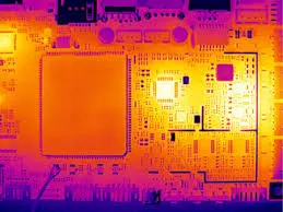
Overheating manifests as via resistance drift or inter-layer shorts, traceable to undersized plating or poor stackup. Engineers troubleshoot by measuring delta T with IR thermography during bench testing. If ampacity falls short, redistribute current via additional vias or thicker planes. Electromigration in high-density arrays signals excessive density; mitigate with copper balancing.
Case studies reveal that hybrid via strategies, combining microvias with larger blind vias, optimize power delivery in consumer electronics. Adhering to J-STD-001 for assembly processes prevents post-process degradation.
Conclusion
Mastering microvia current carrying capacity is vital for reliable HDI PCBs, where ampacity directly governs power delivery and thermal stability. By applying IPC-2152 principles, engineers calculate safe limits considering geometry and environment. Best practices like via paralleling and simulation ensure efficiency without compromising density. Prioritizing these elements yields designs that withstand operational stresses, supporting innovation in compact electronics.
FAQs
Q1: What factors most influence microvia current carrying capacity?
A1: Microvia ampacity depends on plating thickness, via diameter, aspect ratio, and board stackup. Thinner plating increases resistance, concentrating heat, while proximity to planes aids dissipation. IPC-2152 charts guide adjustments for temperature rise. Engineers must model these for accurate power delivery predictions, avoiding overdesign.
Q2: How does IPC-2152 apply to microvia power delivery?
A2: IPC-2152 provides nomographs for conductor capacity, extended to microvias via plating cross-section and thermal factors. It accounts for external versus internal positions, recommending derating for HDI. Use it with simulations for precise ampacity in power nets. This ensures safe current handling without excessive heating.
Q3: Why is microvia thermal management critical in HDI designs?
A3: Microvias generate localized heat due to high current density, risking reliability failures like cratering. Effective management involves via arrays, fillers, and copper planes for dissipation. Balanced stackups prevent warpage. Proper strategies maintain efficient power delivery across layers.
Q4: Can multiple microvias improve ampacity for high-power applications?
A4: Yes, paralleling microvias proportionally increases total current carrying capacity while distributing thermal load. Space them to avoid interference, per HDI rules. This approach excels in power delivery to ICs, validated through thermal modeling. It outperforms single large vias in dense layouts.
References
IPC-2152 — Standard for Determining Current Carrying Capacity in Printed Board Design. IPC, 2009
IPC-2226 — Design Standard for High Density Interconnect (HDI). IPC, 2003
J-STD-001G — Requirements for Soldered Electrical and Electronic Assemblies. IPC, 2011


