ALLPCB


Introduction
Creepage distance and pollution degree are fundamental concepts in PCB design that directly influence electrical safety and reliability. Creepage distance refers to the shortest path along the surface of an insulating material between two conductive parts, while pollution degree classifies the environmental contamination levels that can compromise insulation performance. In PCB applications, particularly those operating under high voltages or in challenging conditions, these factors determine the minimum spacing required to prevent surface flashover or tracking. Engineers must account for creepage distance pollution degree early in the design process to comply with safety standards and ensure long-term functionality. Failure to do so can lead to insulation breakdown, equipment failure, or safety hazards. This article explores their definitions, interactions, and practical implications for PCB design.
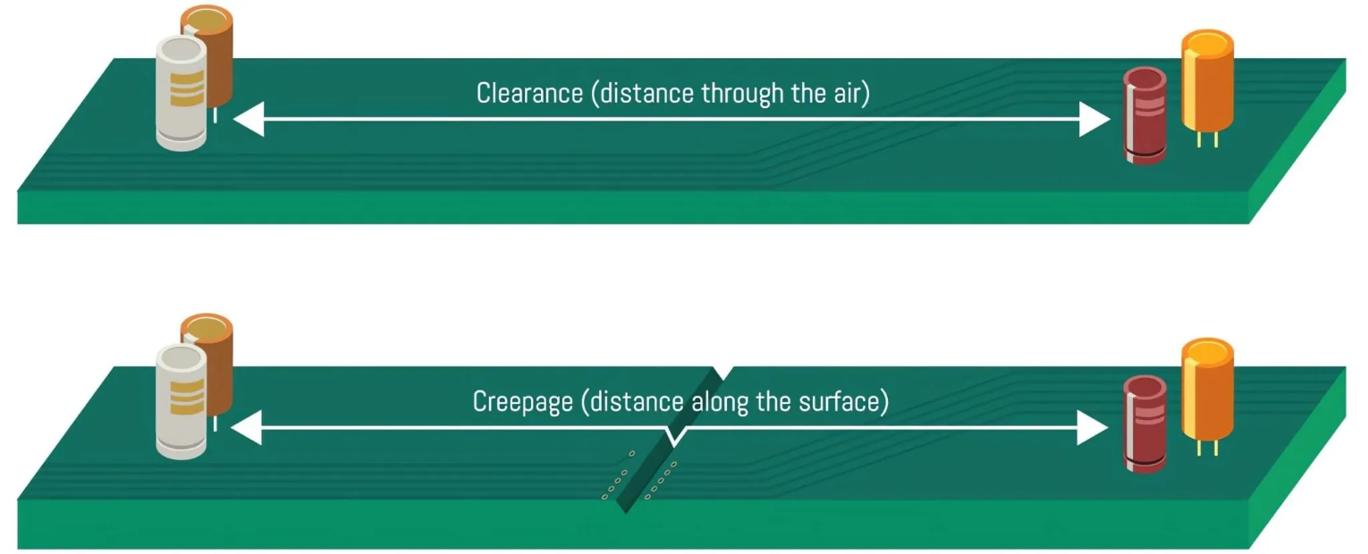
What Is Creepage Distance?
Creepage distance is the measurable path along the PCB surface from one conductor to another, distinct from clearance, which measures the straight-line air gap. This surface path becomes critical because contaminants can bridge the gap and create conductive paths under voltage stress. In PCB design, creepage applies to traces, pads, vias, and components where high potential differences exist. Standards like IEC 60664 provide guidelines for dimensioning creepage based on working voltage and environmental factors. Engineers calculate it during layout to avoid partial discharges or carbon tracking. Proper creepage ensures the PCB withstands operational stresses without degradation.
Why Creepage Distance Matters in PCB Design
Creepage distance prevents electrical tracking, where voltage gradients cause localized heating and carbonization along the insulator surface. This phenomenon is exacerbated in polluted environments, leading to progressive conduction paths that can cause short circuits. For electric engineers designing power supplies or motor drives, inadequate creepage results in field failures, certification delays, or regulatory non-compliance. It also affects thermal management, as wider spacings influence current density and heat dissipation. By prioritizing creepage, designs achieve higher reliability margins across voltage ranges. Ultimately, it balances safety with board compactness for cost-effective manufacturing.
Understanding Pollution Degree
Pollution degree classifies the expected level of dry or wet contamination in the PCB's operating environment, as defined in standards such as IEC 60664. Pollution degree 1 represents clean conditions with no pollution or only dry, non-conductive dust that does not impair insulation. Pollution degree 2 applies to typical indoor settings with non-conductive pollution that may become conductive due to occasional condensation. Higher levels include pollution degree 3 for industrial areas with conductive dust or pollution that becomes conducting from condensation, and pollution degree 4 for severe outdoor exposure with persistent conductivity. The classification guides minimum creepage requirements by accounting for moisture and particles that lower surface resistivity. Accurate assessment prevents overdesign in clean environments or underdesign in harsh ones.
How Pollution Degree Influences Creepage Distance
Pollution degree directly scales the required creepage distance, as higher degrees demand greater surface paths to mitigate tracking risks. In pollution degree 2, occasional moisture films increase conductivity, necessitating spacings that exceed those for pollution degree 1. IEC 60664 outlines dimensioning rules where creepage increases with pollution degree, working voltage, and material group based on comparative tracking index (CTI). For instance, conductive particles in pollution degree 3 environments accelerate carbonization under electric stress. Engineers must evaluate the micro-environment around critical insulation to assign the correct degree. This interaction ensures insulation withstands transient overvoltages without breakdown.
Technical Principles Behind Creepage and Pollution Effects
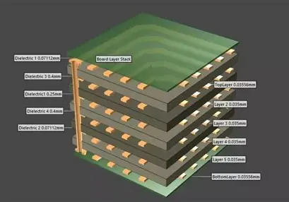
Electrical tracking occurs when ionizable contaminants on the PCB surface form a conductive path under high voltage gradients. Pollution introduces salts, dust, or moisture that lower the surface's insulation resistance, promoting partial discharges. The CTI of the PCB material quantifies resistance to tracking, with higher values allowing shorter creepage for a given pollution degree. Overvoltage categories from IEC 60664 further adjust requirements based on transient exposure. In multilayer boards, internal layers face reduced pollution but still require verification for vias and planes. Understanding these mechanisms enables precise layout optimization.
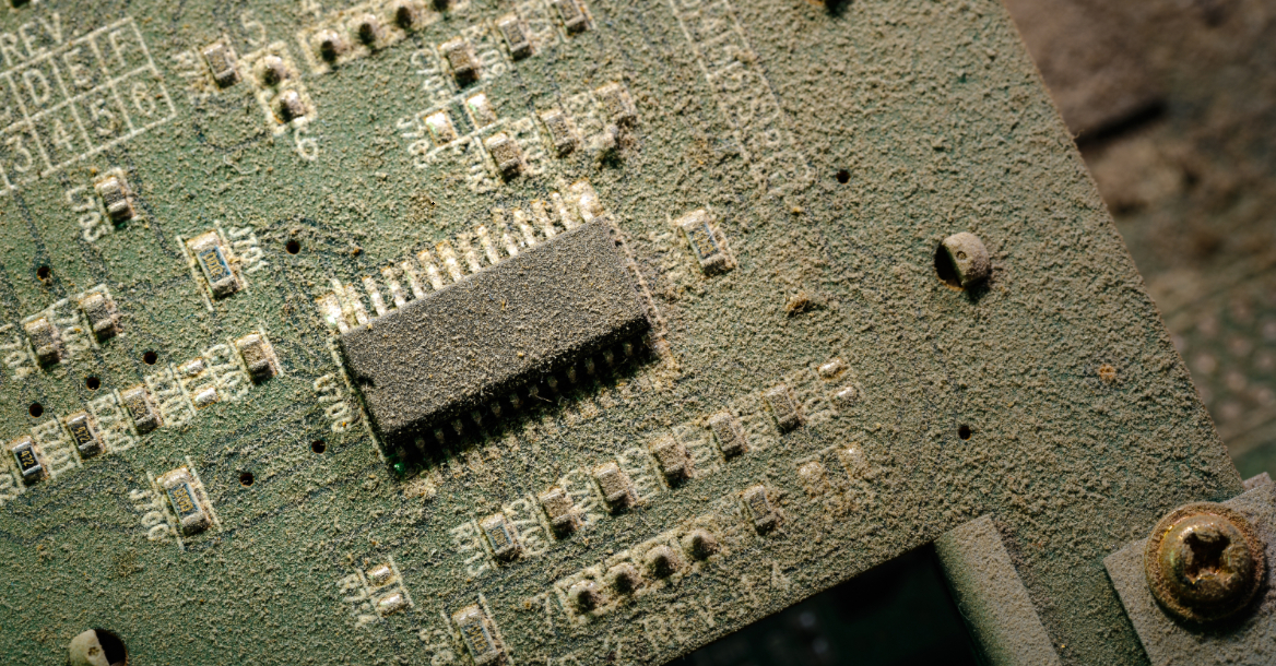
Creepage Distance in Industrial Environments
Industrial environments often qualify as pollution degree 3 due to airborne dust, oils, and humidity fluctuations common in factories or machinery enclosures. Creepage distance industrial environments must accommodate conductive pollution that condenses into tracking paths during operation. Designers increase trace separations or use barriers to meet heightened requirements. Vibration and thermal cycling exacerbate contamination accumulation on surfaces. PCBs in such settings benefit from robust laminates with high CTI. Proactive consideration avoids premature failures in demanding applications.
Best Practices for Pollution Degree PCB Design
Assess the end-use environment to assign pollution degree accurately, consulting IEC 60664 for coordination rules. Select PCB materials with CTI greater than 175 for material group IIIa or better to minimize creepage needs. Apply conformal coatings to reduce effective pollution degree from 3 to 2 or 1 by sealing surfaces against contaminants. Incorporate routing techniques like angled traces or slots to elongate creepage paths without expanding board size. Verify designs through simulation tools modeling voltage distribution and pollution effects. Prototype testing under accelerated pollution confirms compliance before production.
Advanced Techniques to Mitigate Creepage Challenges
Grooves or trenches milled into the PCB surface interrupt potential tracking paths, effectively increasing creepage in constrained areas. Potting compounds encapsulate high-voltage sections, creating a pollution degree 1 micro-environment. Multi-layer stacking isolates sensitive nets internally where pollution impacts are negligible. IPC-2221 provides baseline spacing for external conductors, adjustable for pollution. Combine these with overvoltage derating for robust designs. Iterative DFMEA identifies creepage vulnerabilities early.
Troubleshooting Common Creepage Issues in Polluted Settings
Field returns often trace to underestimated pollution degree, manifesting as charred traces near connectors. Inspect failed boards for carbon tracks correlating to minimum spacings. Recalibrate designs by uprating to pollution degree 3 if industrial deployment is confirmed. Audit supplier material CTI certificates to validate assumptions. Simulate worst-case humidity and dust ingress for virtual validation. Post-mitigation, reliability testing under IEC conditions verifies improvements.
Conclusion
Creepage distance and pollution degree form the cornerstone of safe PCB insulation coordination. By aligning designs with environmental realities and standards like IEC 60664, engineers prevent tracking failures and enhance longevity. Practical strategies such as coatings and path elongation optimize space while upholding safety. In industrial environments, conservative pollution degree assignments yield resilient boards. Mastering these elements elevates PCB performance across applications. Prioritize them from concept through verification for superior outcomes.
FAQs
Q1: What is creepage distance pollution degree?
A1: Creepage distance pollution degree refers to how environmental contamination levels dictate the minimum surface path between conductors on a PCB. Higher pollution degrees require larger creepage to counteract conductive films from dust or moisture. IEC 60664 classifies pollution into degrees 1 through 4, scaling distances accordingly. This ensures insulation reliability under voltage stress. Accurate classification prevents arcing in real-world use.
Q2: How does pollution degree affect PCB design?
A2: Pollution degree in PCB design determines creepage and clearance minima based on expected contaminants. Degree 2 suits offices, while degree 3 fits factories with conductive dust. Higher degrees demand wider spacings to avoid tracking. Coatings can downgrade the effective degree for compact layouts. Engineers reference standards for precise implementation.
Q3: What are creepage distance requirements per IEC 60664?
A3: IEC 60664 specifies creepage distances based on working voltage, pollution degree, CTI, and overvoltage category. Tables guide dimensioning for safe insulation coordination. Factors like altitude correction apply for elevated installations. Printed wiring benefits from reduced values under low pollution. Compliance ensures product certification.
Q4: How to handle creepage distance in industrial environments?
A4: Creepage distance industrial environments assumes pollution degree 3, requiring extended surface paths for dusty, humid conditions. Use high-CTI laminates and protective enclosures. Slots or barriers elongate paths effectively. Verify through environmental testing. This approach maintains safety and reliability.
References
IEC 60664-1:2020 — Insulation coordination for equipment within low-voltage systems – Part 1: Principles, requirements and tests. IEC, 2020
IPC-2221B — Generic Standard on Printed Board Design. IPC, 2012
IEC 60664-3 — Insulation coordination for equipment within low-voltage systems – Part 3: Use of coatings to achieve insulation coordination. IEC, 2020