ALLPCB


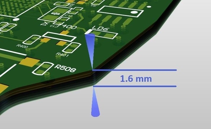
If you're designing a high-current PCB that needs to handle 20A, one of the first things to figure out is the minimum trace width. For a 20A current on a standard PCB with 1 oz copper and a 10°C temperature rise, you’ll typically need a trace width of about 5.2 mm (or 205 mils) on an external layer, based on IPC-2221 standards. This is just a starting point, though—factors like copper thickness, temperature rise limits, and whether the trace is on an internal or external layer will affect the final width. In this guide, we’ll break down the process of calculating trace width for high-current designs, explore key design rules, and provide practical tips to ensure your PCB can safely carry 20A without overheating or failing.
Why Trace Width Matters in High-Current PCB Design
When designing a PCB for high currents like 20A, trace width is critical. A trace that’s too narrow can’t handle the current without overheating, which may lead to performance issues, delamination, or even complete failure of the board. The goal is to calculate a width that keeps the temperature rise within safe limits while ensuring the PCB remains reliable over time. This involves balancing factors like current carrying capacity, copper thickness, and environmental conditions.
In high-current designs, heat is the enemy. As current flows through a trace, it generates heat due to the resistance of the copper. If the trace is too thin, the resistance increases, leading to more heat and a higher risk of damage. That’s why standards like IPC-2221 exist—they provide guidelines to help designers calculate safe trace widths based on current, temperature rise, and other parameters.

Understanding PCB Current Carrying Capacity
Before diving into calculations, let’s define PCB current carrying capacity. This term refers to the maximum amount of current a trace can handle without exceeding a specified temperature rise. The capacity depends on several factors:
- Copper Thickness: Measured in ounces per square foot (oz/ft2), common values are 1 oz (35 μm) and 2 oz (70 μm). Thicker copper can carry more current for the same trace width.
- Trace Width: Wider traces have lower resistance and can handle more current.
- Temperature Rise: The acceptable increase in temperature above ambient conditions, often set at 10°C, 20°C, or 30°C depending on the application.
- Layer Location: External traces (on the top or bottom layer) dissipate heat better than internal traces, so they can be narrower for the same current.
- Ambient Temperature: Higher ambient temperatures reduce the trace’s ability to dissipate heat, requiring wider traces.
For a 20A current, these factors will directly impact the minimum trace width you need. Let’s explore how to calculate it using industry standards.
Using IPC-2221 Standards for Trace Width Calculations
The IPC-2221 standard is a widely accepted guideline for PCB design, including trace width calculations for current carrying capacity. It provides charts and formulas to determine the minimum trace width based on current, copper thickness, and temperature rise. While newer standards like IPC-2152 offer more detailed data, IPC-2221 remains a go-to reference for many designers due to its simplicity and long-standing use.
According to IPC-2221, the relationship between current, trace width, and temperature rise is based on empirical data. The standard assumes a specific set of conditions, such as a certain ambient temperature and no forced cooling. Here’s a step-by-step approach to using IPC-2221 for a 20A design:
- Determine the Current: In this case, it’s 20A.
- Select Copper Thickness: Common options are 1 oz or 2 oz copper. For high-current designs, 2 oz copper is often preferred as it reduces the required trace width.
- Choose Temperature Rise: A 10°C rise is a common starting point for conservative designs, though 20°C or 30°C may be acceptable for less critical applications.
- Identify Layer Location: External layers can handle more current than internal ones due to better heat dissipation.
- Refer to IPC-2221 Charts or Formulas: Use the standard’s data to find the required width. Many online tools are based on these charts and can automate the process.
For example, for 20A on an external layer with 1 oz copper and a 10°C temperature rise, IPC-2221 suggests a trace width of approximately 5.2 mm (205 mils). If you switch to 2 oz copper, the width drops to about 2.6 mm (102 mils) under the same conditions. This shows how much copper thickness impacts design constraints.
Related Reading: The Ultimate Guide to PCB Trace Width for Beginners

Step-by-Step Guide to Calculating Minimum Trace Width for 20A
Let’s walk through a practical example of calculating the minimum trace width for a 20A current on a PCB. We’ll assume standard conditions and use both manual calculations and online tools for accuracy.
Step 1: Define Design Parameters
- Current: 20A
- Copper Thickness: 2 oz (70 μm)
- Temperature Rise: 10°C
- Layer: External
- Ambient Temperature: 25°C
Step 2: Use IPC-2221 Data
Based on IPC-2221 charts, for 20A with 2 oz copper on an external layer and a 10°C rise, the required trace width is approximately 2.6 mm (102 mils). This width ensures the trace won’t overheat under the specified conditions.
Step 3: Verify with a PCB Trace Width Calculator
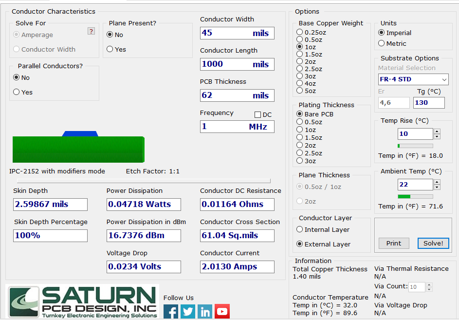
Manual calculations can be time-consuming, and errors can creep in. That’s where a PCB trace width calculator comes in handy. These tools use IPC-2221 or IPC-2152 data to quickly provide accurate results. Simply input the current (20A), copper thickness (2 oz), temperature rise (10°C), and layer type (external), and the calculator will output the minimum trace width. Most calculators confirm the 2.6 mm width for this scenario.
Step 4: Adjust for Real-World Conditions
The calculated width assumes ideal conditions. If your PCB operates in a hotter environment (say, 40°C ambient), or if there’s limited airflow, you may need a wider trace to compensate. Similarly, if the trace is on an internal layer, increase the width by about 50% due to poorer heat dissipation—resulting in a width of around 3.9 mm for 2 oz copper at 20A.
High Current PCB Design Rules for 20A Applications
Beyond calculating trace width, high-current PCB design involves following specific rules to ensure reliability and safety. Here are some essential guidelines for designing a PCB to handle 20A:
- Use Thicker Copper: Opt for 2 oz copper or higher instead of the standard 1 oz. This reduces trace width requirements and improves current carrying capacity. For 20A, 2 oz copper cuts the trace width nearly in half compared to 1 oz.
- Minimize Trace Length: Shorter traces have lower resistance, reducing voltage drop and heat generation. Keep high-current paths as direct as possible.
- Add Copper Pours: For very high currents, consider using copper pours or planes instead of single traces. This spreads the current over a larger area, reducing heat buildup.
- Account for Vias: Vias in high-current paths add resistance and can become hotspots. Use multiple vias in parallel or larger vias to reduce their impact. For 20A, a single 0.3 mm via won’t suffice—opt for several vias or a larger diameter.
- Ensure Proper Spacing: High currents often come with higher voltages, so maintain adequate clearance between traces to prevent arcing. IPC-2221 provides spacing guidelines based on voltage levels.
- Consider Thermal Management: Add heat sinks, thermal vias, or forced cooling if the PCB will operate in a confined space or high ambient temperature.
Following these high current PCB design rules ensures your board can handle 20A without risking failure or overheating.
2 oz Copper Trace Width for 20A: Why It’s a Popular Choice
When designing for high currents like 20A, 2 oz copper is often the go-to choice. Why? It offers a good balance between performance and manufacturability. With 2 oz copper, the trace width for 20A drops to around 2.6 mm on external layers (at a 10°C rise), compared to 5.2 mm with 1 oz copper. This narrower width saves board space, which is critical in compact designs.
Additionally, 2 oz copper is widely supported by most PCB fabrication houses and doesn’t significantly increase costs compared to thicker options like 3 oz or 4 oz. It also handles heat better, reducing the risk of thermal issues in high-current applications. For many engineers, 2 oz copper trace width strikes the perfect balance for 20A designs.
Common Challenges in High-Current PCB Design
Designing a PCB for 20A isn’t without challenges. Here are some common issues and how to address them:
- Space Constraints: Wider traces take up more room, which can be problematic in dense layouts. Using 2 oz copper or higher can help reduce width requirements. Alternatively, consider multi-layer boards to distribute current across layers.
- Heat Dissipation: High currents generate heat, especially in confined spaces. Incorporate thermal vias, heat sinks, or wider traces to manage temperature rise.
- Voltage Drop: Long traces cause voltage drops due to resistance, which can affect performance. Keep high-current traces short and wide, and use thicker copper to minimize resistance.
- Fabrication Limits: Very wide traces or thick copper may exceed the capabilities of some manufacturers. Always check fabrication guidelines before finalizing your design.
Tools and Resources for Trace Width Calculations
Calculating trace width manually using charts can be tedious and error-prone. Fortunately, several online tools simplify the process by automating calculations based on IPC standards. The PCB trace width calculator allows you to input parameters like current, copper thickness, and temperature rise to get instant results. Many also account for internal versus external layers and other variables.
Additionally, PCB design software often includes built-in calculators or constraint managers that enforce trace width rules during layout. Using these tools ensures accuracy and saves time, especially for complex designs handling 20A or more.
Final Thoughts on High-Current PCB Design
Designing a PCB to handle 20A requires careful attention to trace width, copper thickness, and thermal management. By following IPC-2221 guidelines and using tools like PCB trace width calculators, you can determine the minimum trace width—such as 2.6 mm for 2 oz copper on an external layer with a 10°C rise—and ensure your design is safe and reliable. High current PCB design rules, like minimizing trace length and adding thermal relief, further enhance performance.
Whether you’re working on power electronics, automotive systems, or industrial equipment, understanding PCB current carrying capacity is essential. With the right approach, you can create a high-current PCB that meets your needs without compromising on safety or efficiency. Stick to thicker copper like 2 oz for better results, and always double-check your calculations with trusted tools or standards.