ALLPCB


Introduction
PCB routing forms the backbone of any printed circuit board design, directly influencing electrical performance, manufacturability, and long-term reliability. Engineers must carefully plan trace paths to connect components while minimizing signal degradation and manufacturing defects. Effective PCB routing strategies balance space constraints with electrical requirements, ensuring signals propagate with integrity across the board. As designs grow more complex with higher component densities, mastering these techniques becomes essential for electric engineers tackling modern applications. This article explores proven PCB routing strategies, compares autorouting versus manual routing, and delves into critical aspects like trace width calculation and via selection for routing. By applying these principles, designers can achieve efficient, high-performance PCBs.
Understanding PCB Routing and Its Critical Role
PCB routing involves creating conductive paths, or traces, between component pads on a circuit board to establish electrical connectivity. These traces carry signals, power, and ground, and their layout must account for factors like impedance control, crosstalk reduction, and thermal management. Poor routing can lead to signal reflections, electromagnetic interference, or mechanical stress failures during operation. In high-speed designs, routing decisions directly impact timing budgets and overall system performance. Industry standards like IPC-2221 provide foundational guidelines for routing geometry, ensuring consistency across designs. Ultimately, thoughtful routing enhances board yield and reduces iteration costs in production.
Routing matters because it bridges schematic intent with physical realization. Engineers face trade-offs between minimizing trace lengths for low latency and allocating space for wider traces to handle current without excessive heating. Compliance with standards prevents common pitfalls, such as inadequate clearance that could cause shorts or arcing. For electric engineers, routing proficiency translates to faster design cycles and reliable prototypes.
Core Principles of Effective PCB Routing
Successful PCB routing starts with understanding electrical characteristics of traces. Traces act as transmission lines at high frequencies, where controlled impedance prevents reflections and maintains signal quality. Engineers prioritize shortest paths for critical signals while grouping related nets to reduce noise coupling. Ground planes adjacent to signal layers provide return paths, minimizing loop inductance. Mechanical aspects, like avoiding sharp bends that concentrate stress, also play a role in durability.
Power integrity requires dedicated planes or wide traces to distribute current evenly, preventing voltage drops. Thermal dissipation influences routing, as dense trace areas can trap heat. Logical layering schemes separate analog, digital, and power sections to isolate noise sources. Adhering to design rules derived from IPC-2221 ensures traces meet minimum widths and spacings for given voltage levels. These principles form the foundation for all PCB routing strategies.
Autorouting vs Manual Routing: Choosing the Right Approach
Autorouting automates trace placement based on predefined rules, speeding up initial layouts for simple boards. It excels in low-density designs where connectivity is straightforward, quickly filling available space without human intervention. However, autorouters often struggle with high-speed signals, producing suboptimal paths that violate length matching or impedance targets. They may generate excessive vias or ignore manufacturing constraints, leading to redesigns.
Manual routing offers precise control, allowing engineers to optimize for performance metrics like differential pair symmetry. Experienced designers route critical nets first, using techniques like 45-degree bends to reduce reflections. This method shines in complex boards, where visual inspection reveals potential issues early. While time-intensive, manual routing aligns closely with simulation results and standards compliance. A hybrid approach, starting with autorouting and refining manually, combines efficiency with quality for most projects.
Trace Width Calculation: Ensuring Current Capacity and Reliability
Trace width calculation determines the conductor size needed to carry specified currents without exceeding allowable temperature rises. Factors include copper thickness, ambient temperature, and board stackup, as narrower traces increase resistance and heat generation. Engineers use empirical charts and formulas from IPC-2221 to select widths that balance space and thermal performance. For power traces, wider dimensions prevent hotspots that could delaminate the board over time.
In multilayer boards, internal layers may require adjustments due to poorer heat dissipation compared to external ones. Signal traces prioritize impedance over current, often using thinner widths with precise spacing. Iterative verification through thermal simulations refines calculations, ensuring margins for worst-case scenarios. Proper sizing supports overall power distribution integrity.
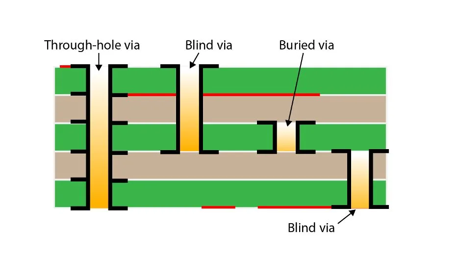
Via Selection for Routing: Optimizing Inter-Layer Connections
Vias serve as vertical interconnects between layers, and their selection impacts routing density and signal integrity. Through-hole vias penetrate the entire board, suitable for simple designs but consuming more space in dense layouts. Blind and buried vias connect only specific layers, enabling tighter routing by freeing surface area. Microvias, with diameters under 150 microns, suit high-density applications per IPC-2226 guidelines.
Via size affects inductance and capacitance; smaller ones preserve high-frequency performance but demand advanced fabrication. Placement strategy minimizes stub lengths for better impedance matching. Aspect ratios, typically limited to 8:1 or less, ensure reliable plating. Selecting the right via type streamlines high-density PCB routing while controlling costs.
High-Density PCB Routing Strategies
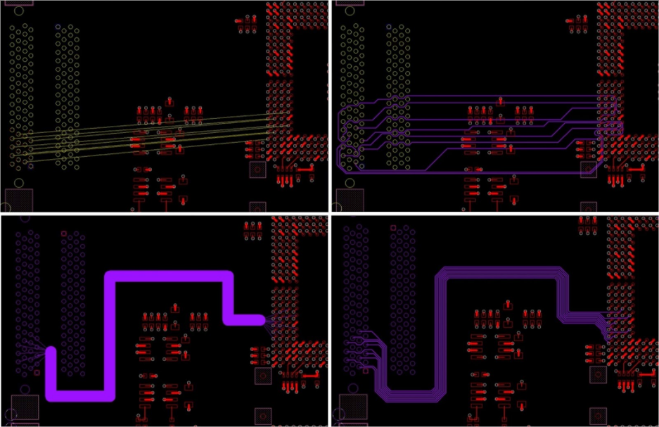
High-density PCB routing demands innovative techniques to pack traces into constrained spaces without compromising function. Layer staggering alternates signal directions to maximize utilization, while fanouts from fine-pitch components use dedicated via grids. Differential pairs require constant spacing and length matching to preserve common-mode rejection. Embedded components or cavities reduce top-layer congestion.
Microvia staggering, as outlined in IPC-2226, builds complex interconnects without excessive drill counts. Power and ground planes split strategically to isolate domains. Routing high-speed signals on inner layers with solid references cuts crosstalk. These strategies enable compact designs for portable electronics and servers.
Best Practices for Implementation
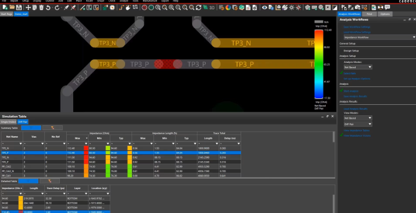
Start routing with a clear hierarchy: critical high-speed nets first, followed by power, then general signals. Enforce design rules for minimum clearance and width throughout. Use length-tuning tools for clock lines to meet setup times. Verify routing completeness with design rule checks and electrical rule checks.
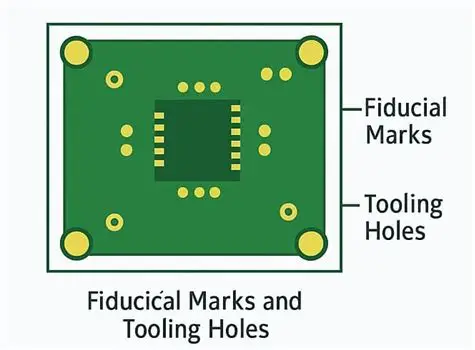
Incorporate test points and fiducials for manufacturability. Simulate signal integrity post-routing to catch issues like ringing. Document deviations with engineering justifications. These practices, aligned with IPC-6012 performance specs, yield robust boards ready for production.
Conclusion
Mastering PCB routing strategies empowers electric engineers to create efficient, reliable designs that meet demanding specifications. Balancing autorouting versus manual routing, precise trace width calculation, thoughtful via selection for routing, and specialized high-density PCB routing techniques ensures optimal outcomes. Adhering to standards like IPC-2221 and IPC-2226 minimizes risks and enhances performance. By prioritizing electrical, thermal, and mechanical principles, designers reduce iterations and accelerate time-to-market. Implementing these top strategies elevates PCB quality across applications.
FAQs
Q1: What are the main PCB routing strategies for high-speed signals?
A1: PCB routing strategies for high-speed signals emphasize controlled impedance traces, symmetric differential pairs, and minimal vias. Route over continuous ground planes to reduce inductance, and use 45-degree bends instead of 90-degree corners to avoid reflections. Length matching ensures timing alignment, while spacing rules per IPC-2221 prevent crosstalk. These approaches maintain signal integrity in dense layouts.
Q2: How does autorouting compare to manual routing in complex designs?
A2: Autorouting vs manual routing shows autorouters efficient for basic connectivity but inadequate for complex high-density PCB routing. Manual routing provides control over impedance and length, essential for performance-critical nets. Hybrids leverage autorouter speed with manual refinement. Electric engineers prefer manual for high-reliability boards to comply with standards.
Q3: What factors influence trace width calculation?
A3: Trace width calculation depends on current capacity, copper thickness, temperature rise limits, and layer position. IPC-2221 guidelines offer charts for external and internal traces, factoring ambient conditions. Wider traces suit power delivery, while signals balance with spacing. Simulations verify thermal performance.
Q4: How to choose via selection for routing in multilayer boards?
A4: Via selection for routing considers density, cost, and signal needs: through-hole for general use, blind/buried for space savings, microvias for HDI. Limit aspect ratios for plating reliability, and position to minimize stubs. IPC-2226 specifies microvia rules for high-density PCB routing.
References
IPC-2221B — Generic Standard on Printed Board Design. IPC, 2003
IPC-2226A — Sectional Design Standard for High Density Interconnects. IPC, 2002
IPC-6012F — Qualification and Performance Specification for Rigid Printed Boards. IPC, 2023