 ALLPCB


Introduction
Electronic hobbyists often start with breadboards for prototyping circuits, but transitioning to custom printed circuit boards unlocks more reliable and compact designs. PCB layout forms the core of this process, turning schematic diagrams into physical boards ready for fabrication. In 2025, a wealth of free PCB layout courses and online PCB tutorials makes learning accessible without financial barriers. These resources cater to beginners, offering step-by-step guidance on essential skills. Whether building a simple LED driver or a microcontroller project, mastering PCB design online empowers hobbyists to create professional-grade electronics. This article explores key principles, best practices, and where to find high-quality free training.
What Is PCB Layout and Why Does It Matter for Hobbyists?
PCB layout involves arranging components on a board and routing conductive traces to connect them according to the circuit schematic. This step follows schematic capture and precedes manufacturing, ensuring signals flow correctly while minimizing interference. For electronic hobbyists, effective layout prevents issues like short circuits, overheating, or poor performance that plague hand-wired prototypes. It enables smaller, durable designs suitable for enclosures or wearables. Industry standards like IPC-2221 guide layout decisions on trace widths, spacings, and material choices to achieve reliability. Learning PCB design online equips hobbyists with these fundamentals, bridging the gap from theory to tangible projects.
Poor layout can lead to signal crosstalk or excessive power loss, compromising project success. Hobbyists benefit from layouts that support easy assembly and testing, reducing iteration time. Free PCB layout courses emphasize these aspects, teaching how to balance aesthetics with functionality. As projects grow complex, such as adding microcontrollers or sensors, solid layout skills become indispensable. Online electronics courses often highlight real-world applications, showing how layout impacts battery life or electromagnetic compatibility.
Core Technical Principles of PCB Layout
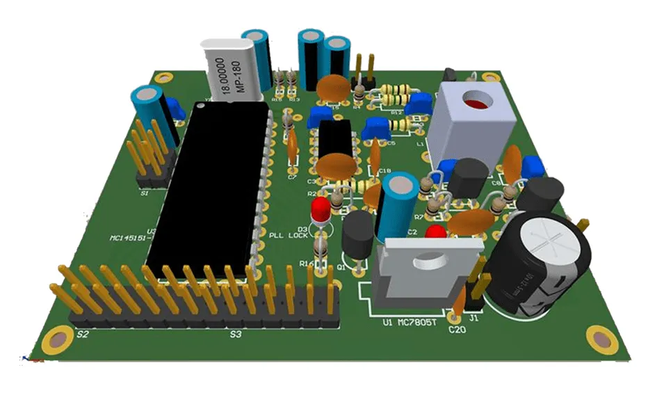
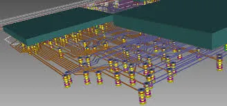
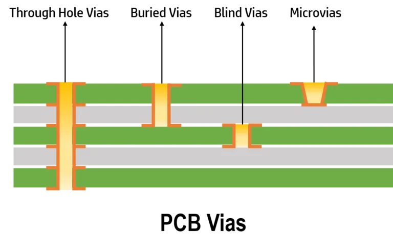
Understanding layer stackup starts the layout process, where hobbyists decide between single-sided, double-sided, or multilayer boards based on complexity. Single-layer suits ultra-simple circuits, while double-layer handles most hobby projects with ground planes for noise reduction. Traces carry current and signals, sized according to current load and voltage drop calculations outlined in standards like IPC-2221. Wider traces reduce resistance for power lines, narrower ones suffice for signals. Vias connect layers, placed strategically to avoid clutter. Proper clearance prevents arcing, especially in high-voltage sections.
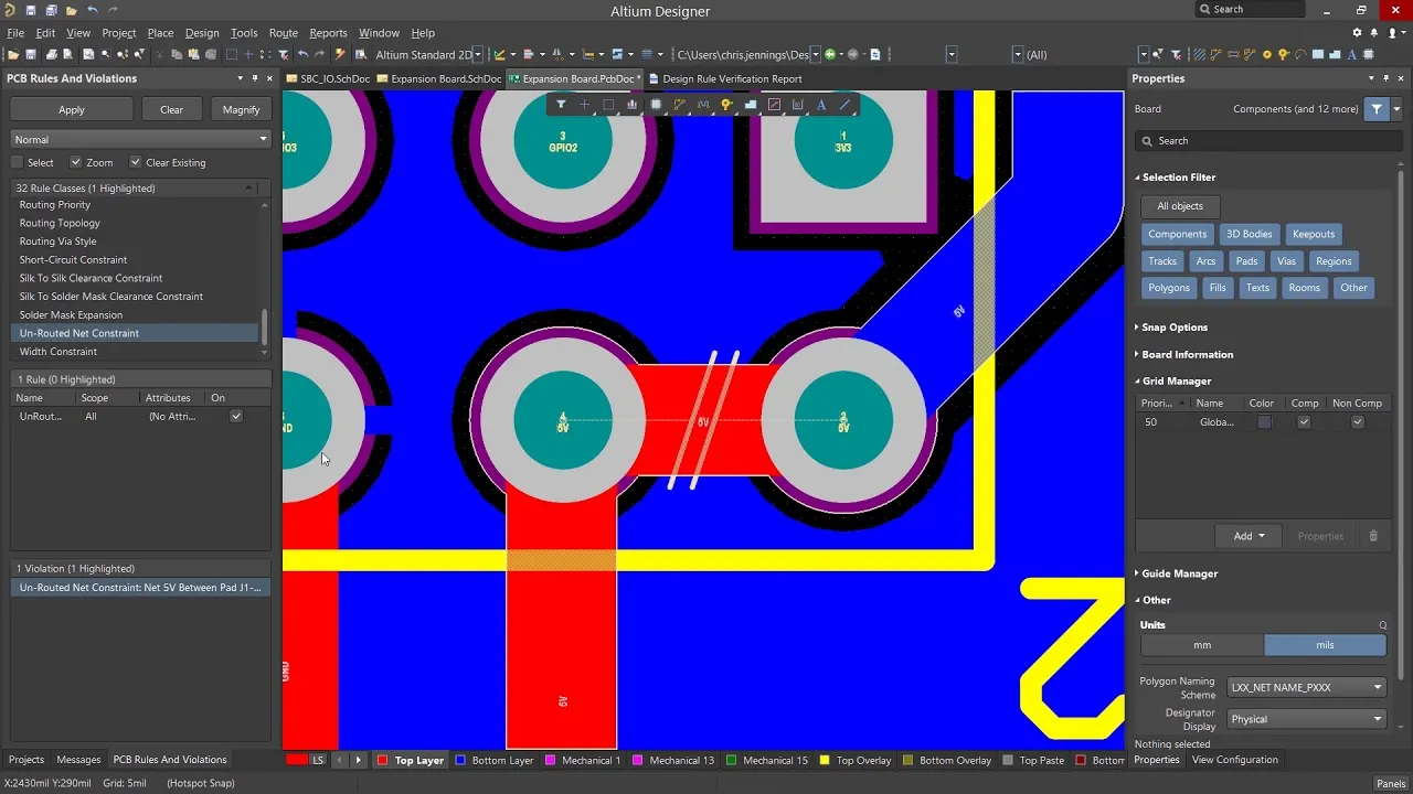
Component placement prioritizes signal flow, grouping related parts like decoupling capacitors near ICs to minimize loop inductance. Analog and digital sections separate to curb noise coupling. Thermal management considers heat dissipation, positioning high-power components away from sensitive areas. Ground planes provide return paths, improving integrity. Design rule checks verify minimum widths, spacings, and overlaps before export. These principles ensure boards meet performance goals without fabrication issues.
Routing follows placement, using autorouters judiciously while manual tweaks refine paths. Avoid 90-degree bends, opting for 45-degree angles to reduce reflections. Differential pairs for high-speed signals maintain equal lengths and spacing. Power distribution networks deliver stable voltage, often via polygons. Silkscreen adds labels for assembly ease. Adhering to IPC-7351 for land patterns ensures solder joints form reliably during hand assembly.
Finding Free PCB Layout Courses and Online Tutorials in 2025
Numerous platforms host free PCB layout courses tailored for beginners, searchable with terms like free PCB layout courses or online PCB tutorials. Video series break down schematic-to-layout workflows, often with screen recordings of design environments. University open courseware provides lecture notes and simulations, ideal for structured learning. Community-driven sites offer project-based tutorials, from blinky lights to sensor interfaces. Forums host Q&A threads where hobbyists share layouts for feedback. In 2025, updated content incorporates modern practices like flexible boards or embedded passives.
PCB software training abounds in short modules, covering import, placement, and routing basics. Look for series progressing from single-layer to four-layer designs. Interactive quizzes reinforce concepts like via fencing for shielding. Downloadable example files allow practice without starting from scratch. Aggregator sites curate top online electronics courses, filtering by skill level. Consistency across resources builds confidence quickly.
Best Practices for Learning PCB Design Online
Start with foundational online PCB tutorials focusing on schematic entry before layout, ensuring logical circuit flow. Practice on simple projects like power supplies to master placement grids and snap tools. Gradually tackle mixed-signal boards, applying separation techniques. Verify designs with electrical rule checks for shorts or unconnected nets. Export Gerber files and review previews for errors. Iterate by fabricating low-cost prototypes to learn from real failures.
Join discussions in hobbyist communities to review peers' layouts, gaining diverse insights. Track progress with a portfolio of boards, noting improvements in density or cleanliness. Combine video learning with written guides for reinforcement. Allocate time weekly, aiming for one complete layout per session. Reference standards sporadically, like IPC-A-600 for visual acceptability post-fabrication. This methodical approach turns novices into capable designers.
Optimize learning by simulating layouts virtually before physical builds, catching issues early. Focus on manufacturability, such as annular ring sizes for drill accuracy. Document decisions in notes for future reference. Experiment with design variations to understand trade-offs, like trace length versus impedance. Free resources evolve, so bookmark promising series for 2025 updates. Patience yields polished results.
Common Challenges in PCB Layout and Troubleshooting Tips
Hobbyists often overcrowd boards, leading to routing congestion; counter this by rough placement sketches first. Signal integrity issues arise from long traces; shorten paths or add shielding. Power noise affects stability; employ star grounding or planes. Thermal hotspots demand copper pours or vias for heat spreading. DRC violations signal rule breaches; adjust clearances iteratively.
Vias farm out for EMI control, encircling sensitive nets. Solder mask bridges fixed by panelization tweaks. Learning curve steepens with high-density interconnects; scale gradually. Troubleshooting involves scope probing prototypes for anomalies. Online PCB tutorials address these with case examples. Persistence refines intuition over time.
Conclusion
Mastering PCB layout through free resources transforms hobbyist projects from fragile prototypes to robust electronics. Key principles like strategic placement, proper routing, and standard adherence ensure success. Free PCB layout courses, online PCB tutorials, and PCB software training provide the tools needed in 2025. Best practices emphasize practice, verification, and community engagement. Hobbyists gain independence, iterating designs efficiently. Start today to elevate your electronics journey.
FAQs
Q1: What are the best free PCB layout courses for electronic hobbyists?
A1: Free PCB layout courses on video platforms and open aggregators offer step-by-step guidance from schematics to Gerbers. They cover placement, routing, and basic simulations suitable for beginners. Search for 2025 updates focusing on double-layer boards. Practice with provided examples to build skills quickly. These resources align with hobby needs without overwhelming theory.
Q2: How can I learn PCB design online without prior experience?
A2: Begin with online PCB tutorials emphasizing visual workflows and simple projects. Progress through modules on layers, traces, and vias. Use free viewers for Gerber inspection. Communities provide feedback on your layouts. Consistent 30-minute sessions yield results in weeks. Incorporate standards like IPC-2221 for credible designs.
Q3: Where to find PCB software training for free in 2025?
A3: PCB software training hides in short series on tutorial hubs and forums. Look for hands-on routing and DRC demos. University archives offer advanced overviews. Hobby-focused channels update yearly. Download templates to experiment safely. This builds proficiency for personal projects efficiently.
Q4: Are online electronics courses effective for PCB layout basics?
A4: Yes, online electronics courses integrate PCB layout with circuit theory effectively. They teach practical routing and placement for hobby applications. Interactive elements like quizzes aid retention. Real project walkthroughs demonstrate full flows. Track 2025 content for emerging trends. Results appear in functional prototypes.
References
IPC-2221B - Generic Standard on Printed Board Design. IPC, 2003
IPC-A-600M - Acceptability of Printed Boards. IPC, 2025
IPC-7351B - Generic Requirements for Surface Mount Design and Land Pattern Standard. IPC, 2010
J-STD-001J - Requirements for Soldered Electrical and Electronic Assemblies. IPC, 2024


