 ALLPCB


Introduction
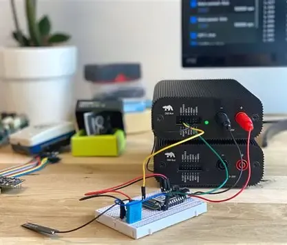
IoT devices integrate sensors, wireless modules, and microcontrollers onto compact printed circuit boards that must operate reliably in diverse environments. Quick turn PCB prototyping IoT enables engineers to validate designs rapidly before scaling to production volumes. This approach supports iterative improvements in power management, signal integrity, and mechanical fit within constrained enclosures. PCB fabrication services IoT must accommodate mixed-signal layouts, RF traces, and flexible substrates while maintaining tight tolerances. Effective PCB assembly prototyping combines surface-mount technology with through-hole components to achieve functional prototypes in days rather than weeks. PCB testing services IoT verify electrical performance, thermal behavior, and environmental resilience at each stage.
Why Quick Turn PCB Prototyping Matters for IoT
IoT applications span industrial monitoring, smart infrastructure, and consumer wearables, each imposing unique requirements on board size, layer count, and material selection. Rapid prototyping cycles allow teams to evaluate antenna performance, power consumption profiles, and electromagnetic compatibility early in development. Design for manufacturing IoT principles guide layout choices that minimize fabrication defects and assembly errors. Shorter lead times reduce overall project risk and accelerate time-to-market for connected products. Engineers can test multiple board revisions against real-world operating conditions without committing to large production runs. This flexibility proves essential when integrating new wireless protocols or optimizing for battery life.
Technical Principles of IoT PCB Prototyping
IoT boards frequently combine high-speed digital circuits with sensitive analog sections and RF paths on the same substrate. Controlled impedance routing, proper grounding strategies, and thermal relief patterns become critical to maintain signal quality. Layer stack-up decisions influence both electrical performance and manufacturability, especially when incorporating blind or buried vias. Material selection balances dielectric properties, thermal conductivity, and moisture absorption to suit the intended operating environment.
Power distribution networks must deliver stable voltage to multiple components while minimizing noise coupling. Decoupling capacitor placement and trace width calculations follow established engineering practices to support varying load currents. Thermal management techniques, including copper pours and thermal vias, address heat generated by processors and power regulators in compact enclosures.
Design for Manufacturing in IoT PCB Development
Design for manufacturing IoT emphasizes panelization strategies, fiducial placement, and solder mask clearances that align with standard fabrication capabilities. Component footprints follow recommended land patterns to ensure reliable solder joints during PCB assembly prototyping. Trace widths, spacing, and via sizes are chosen to match available process tolerances and avoid yield loss. Clearances around mounting holes and edge connectors accommodate mechanical assembly steps without compromising electrical integrity. Early collaboration between design and manufacturing teams identifies potential issues such as insufficient annular rings or unbalanced copper distribution. These considerations reduce the number of prototype iterations required to reach a production-ready layout.
PCB Fabrication and Assembly Processes for IoT
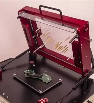
PCB fabrication services IoT begin with photolithography and etching steps that define precise conductor patterns on copper-clad laminates. Drilling operations create through-holes and vias, followed by plating to establish electrical connections between layers. Surface finishes such as immersion silver or electroless nickel immersion gold protect exposed copper and support fine-pitch component attachment. PCB assembly prototyping proceeds with solder paste application via stencil, followed by automated placement of surface-mount devices and reflow soldering. Through-hole components may be inserted manually or via wave soldering depending on board complexity.
Quality checks during assembly include visual inspection and automated optical inspection to detect placement or soldering anomalies before functional testing.
Testing and Quality Assurance in IoT Prototyping
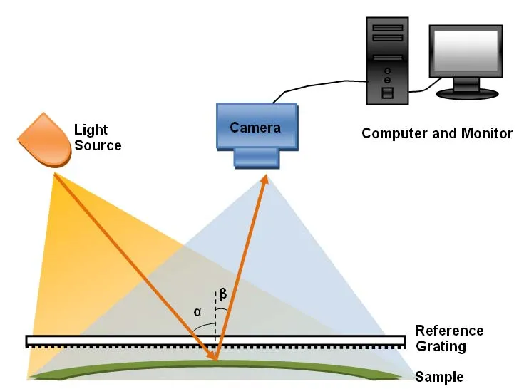
PCB testing services IoT encompass in-circuit testing for opens and shorts, functional verification under simulated operating conditions, and environmental stress screening. Burn-in procedures and thermal cycling help identify latent defects related to material fatigue or connection integrity. RF performance validation measures return loss, insertion loss, and radiated emissions to confirm wireless module compliance with intended protocols.
Acceptance criteria often reference IPC-6012E for rigid board qualification and IPC-A-600K for visual acceptability of printed boards. These standards provide consistent benchmarks for evaluating prototype quality across different fabrication runs.
Best Practices for Efficient IoT PCB Prototyping
Engineers maintain version-controlled design files and comprehensive documentation to support rapid revisions between prototype spins. Standardized test procedures and fixture reuse accelerate validation cycles while preserving traceability. Material lot tracking and process parameter logging facilitate root-cause analysis when issues arise. Regular design reviews incorporate feedback from fabrication and assembly partners to refine layouts for higher yields.
Thermal and mechanical simulations performed early help predict behavior under expected environmental loads, guiding material and layout adjustments before physical builds.
Conclusion
Quick turn PCB prototyping IoT streamlines the path from concept to validated hardware by combining disciplined design practices with responsive fabrication and assembly capabilities. Attention to design for manufacturing IoT principles, combined with thorough PCB testing services IoT, ensures prototypes meet performance and reliability expectations. Structured processes grounded in established industry standards support consistent results across multiple development iterations. Engineers who apply these methods achieve faster design cycles and more robust IoT solutions.
FAQs
Q1: What distinguishes quick turn PCB prototyping IoT from standard board development?
A1: Quick turn PCB prototyping IoT focuses on accelerated fabrication and assembly cycles that deliver functional boards in days, enabling rapid design validation for connected devices. Engineers use these prototypes to test wireless performance, power efficiency, and mechanical integration before committing to volume production. The process emphasizes design for manufacturing IoT guidelines to minimize revisions while maintaining quality.
Q2: How does design for manufacturing IoT improve PCB assembly prototyping outcomes?
A2: Design for manufacturing IoT incorporates panelization, fiducial placement, and land pattern optimization that align with standard assembly equipment capabilities. These choices reduce placement errors and soldering defects during PCB assembly prototyping. The result is higher first-pass yield and fewer costly respins when moving from prototype to production.
Q3: Why are PCB testing services IoT essential during the prototyping phase?
A3: PCB testing services IoT verify electrical continuity, functional operation, and environmental resilience before devices enter field trials. Tests include in-circuit checks, RF characterization, and thermal cycling to identify issues early. Reference standards such as JEDEC J-STD-020E guide moisture sensitivity handling during these evaluations.
Q4: What role does PCB fabrication services IoT play in supporting IoT innovation cycles?
A4: PCB fabrication services IoT provide the foundational boards that integrate sensors, processors, and communication modules into compact, reliable platforms. Fast turnaround allows teams to iterate on antenna layouts, layer stack-ups, and thermal solutions quickly. Consistent quality from these services underpins successful scaling of IoT products.
References
IPC-6012E - Qualification and Performance Specification for Rigid Printed Boards. IPC, 2017
IPC-A-600K - Acceptability of Printed Boards. IPC, 2020
JEDEC J-STD-020E - Moisture/Reflow Sensitivity Classification. JEDEC, 2014


