ALLPCB


Introduction
PCB layout plays a central role in determining the appropriate stencil thickness for solder paste application during surface mount assembly. Engineers must evaluate component density, pad geometries, and spacing early in the design phase to ensure consistent solder paste deposition. Stencil thickness directly influences the volume of paste transferred to each pad, which in turn affects joint reliability and manufacturing yield. When layout features such as fine-pitch components or large thermal pads are present, the selected thickness must balance adequate coverage with the risk of defects. This relationship between layout decisions and stencil parameters forms a critical part of achieving repeatable assembly outcomes.
What Is Stencil Thickness Selection and Why It Matters
Stencil thickness selection refers to the process of choosing the metal foil thickness that controls the amount of solder paste deposited through apertures onto PCB pads. The chosen thickness must align with the specific requirements of the PCB layout to deliver the correct paste volume for each component type. In high-density designs, inadequate thickness can result in insufficient paste for reliable joints, while excessive thickness may cause bridging between closely spaced pads. Industry standards such as IPC-7525 provide guidelines for matching stencil parameters to layout features. Proper selection supports consistent solder paste deposition across production runs and reduces the likelihood of rework or field failures. Engineers therefore treat stencil thickness as an integral design consideration rather than an afterthought.
Technical Principles: How PCB Layout Influences Solder Paste Deposition
The relationship between PCB layout and stencil thickness centers on the volume of solder paste required for each pad. Larger pads or those connected to thermal planes demand greater paste volume, which typically requires a thicker stencil to maintain the correct aspect ratio between aperture opening and foil thickness. Conversely, fine-pitch components with narrow spacing benefit from thinner stencils that reduce the risk of paste bridging during deposition. Component placement density further complicates the decision, as clusters of small devices near larger ones create conflicting volume requirements within the same board area. Layout features such as pad shape, orientation, and proximity to board edges also affect paste release efficiency and must be accounted for when calculating the area ratio. These interactions follow established engineering principles that link geometric layout parameters directly to the mechanics of paste transfer.
Related Reading: Decoding Stencil Thickness: A Comprehensive Guide for PCB Assembly Success
Practical Solutions and Best Practices for Design Considerations
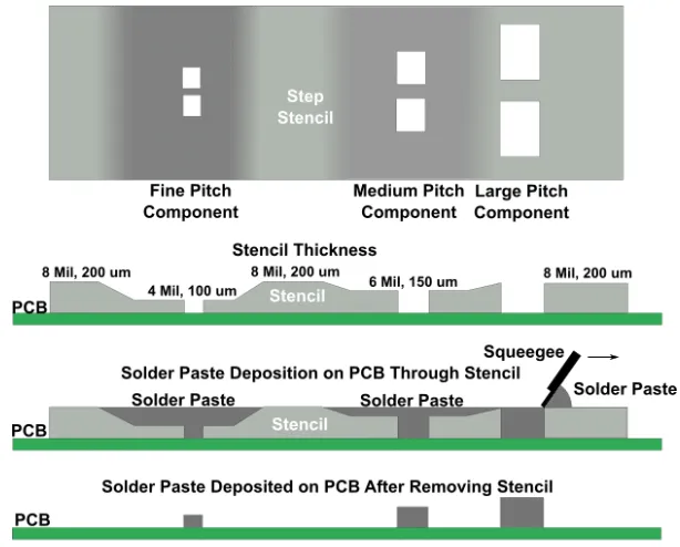
Design teams begin by reviewing the complete component placement and pad layout to identify areas with varying volume needs. They then apply area-ratio calculations to determine a baseline stencil thickness that satisfies the majority of pads while flagging exceptions for special treatment. When fine-pitch devices coexist with standard components, segmented or step-down stencils can be considered to locally adjust thickness without compromising overall board integrity. Engineers also evaluate solder mask defined versus non-solder mask defined pads, because the chosen definition influences the effective aperture size and therefore the required foil thickness. Early collaboration between layout and process engineers helps incorporate these factors before finalizing the design files. Following these steps produces a stencil specification that supports reliable solder paste deposition across the entire assembly.
Related Reading: Step Stencil Thickness: How to Determine the Ideal Value for Your PCB
Troubleshooting Common Issues in Component Placement
When solder paste volume inconsistencies appear during first-article builds, engineers trace the root cause back to specific layout elements. Insufficient paste on thermal pads often stems from an overly thin stencil relative to the pad size and component thermal mass. Bridging between adjacent pads frequently occurs when a thicker stencil is used in regions with tight component placement spacing. In such cases, aperture modifications or localized thickness adjustments are evaluated while preserving the original PCB layout. Systematic review of paste deposit measurements against calculated volumes confirms whether the selected thickness aligns with the actual component placement requirements. This diagnostic approach isolates layout-driven issues and guides targeted corrections without requiring extensive redesign.
Conclusion
PCB layout decisions directly shape the stencil thickness needed for optimal solder paste deposition and long-term joint reliability. By evaluating component placement, pad geometries, and spacing during the design phase, engineers can select a thickness that meets volume requirements while minimizing defect risks. Structured application of area-ratio principles and early process input ensures the chosen stencil supports consistent manufacturing results. These considerations remain essential for achieving high-yield assembly in modern electronic products.
FAQs
Q1: How does PCB layout influence stencil thickness selection?
A1: PCB layout determines the required solder paste volume for each pad through factors such as pad size, spacing, and component density. Engineers calculate area ratios based on these layout features to select a stencil thickness that delivers adequate deposition without causing bridging or insufficient joints. This process ensures the stencil matches the specific design considerations of the board.
Q2: What role does solder paste deposition play in stencil thickness decisions?
A2: Solder paste deposition volume must match the thermal and mechanical needs of each component, which varies according to the PCB layout. A properly chosen stencil thickness maintains the correct paste height and coverage, supporting reliable reflow and minimizing defects related to component placement. Layout analysis therefore guides thickness selection to achieve consistent deposition results.
Q3: Why are design considerations important when choosing stencil thickness?
A3: Design considerations such as fine-pitch spacing and mixed pad sizes create competing requirements for paste volume within a single PCB layout. Addressing these factors early allows engineers to select a stencil thickness that balances coverage across all components while following established assembly guidelines. This approach improves yield and reduces the need for post-design adjustments.
Q4: How can engineers optimize stencil thickness for complex component placement?
A4: Engineers review the full component placement and apply area-ratio calculations to identify regions that need standard or adjusted thickness. When layout features create volume conflicts, they consider aperture modifications or localized stencil changes while maintaining overall board integrity. This methodical evaluation ensures the final thickness supports reliable solder paste deposition throughout the assembly process.
References
IPC-7525B — Stencil Design Guidelines. IPC, 2019
J-STD-005A — Requirements for Soldering Pastes. IPC, 2012
IPC-A-610G — Acceptability of Electronic Assemblies. IPC, 2017