 ALLPCB


Introduction
The automotive industry faces increasing demands for efficient power handling as electric vehicles proliferate and traditional engines incorporate advanced electronics. Heavy copper PCB automotive designs emerge as critical components to manage high currents and dissipate heat effectively in these systems. Engineers rely on these boards for applications ranging from battery management to power inversion, ensuring reliability under harsh operating conditions like vibration and temperature extremes. PCB for electric vehicles must support rapid power delivery while minimizing losses, making heavy copper layers essential for performance. Automotive electronics benefit from the mechanical robustness these PCBs provide, reducing failure risks in dynamic environments. This article explores practical applications, design strategies, and troubleshooting insights for heavy copper implementations.
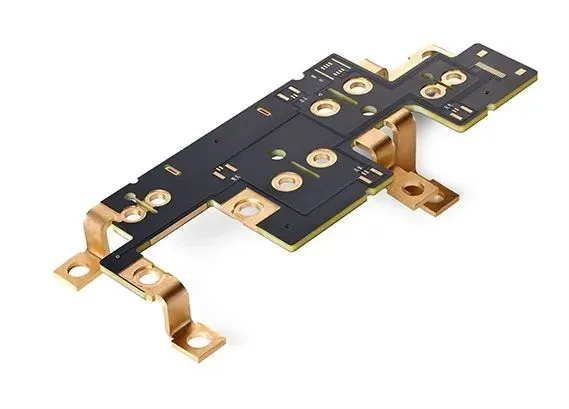
What Are Heavy Copper PCBs and Their Relevance to Automotive
Heavy copper PCBs feature copper layers thicker than standard 1 or 2 ounce per square foot weights, typically starting from 3 ounces or more to handle elevated current densities. In automotive contexts, this thickness enables superior current carrying capacity without excessive trace widths, optimizing space in compact modules. The enhanced thermal conductivity of thicker copper aids in spreading heat from power devices, preventing hotspots that could degrade components. Automotive electronics demand such capabilities due to high power requirements in electrification trends. These boards also offer greater mechanical strength, resisting warpage and delamination during thermal cycling common in vehicle operation. Engineers specify heavy copper for reliability in mission-critical systems where failure impacts safety.
The distinction from standard PCBs lies in manufacturing and performance trade-offs. Thicker copper requires specialized etching to maintain trace integrity, yet it supports higher amperage loads critical for automotive power distribution. Vibration resistance improves with the added mass and rigidity, aligning with rigorous environmental stresses in vehicles.
Key Applications of Heavy Copper PCBs in Automotive Electronics
Battery management system PCBs represent a primary use case for heavy copper in electric vehicles. These boards monitor cell voltages, balance charges, and manage thermal runaway risks, often carrying substantial currents between cells and the main bus. Heavy copper traces minimize resistive losses, ensuring accurate sensing and efficient power flow even under high loads. Troubleshooting tip: Monitor for uneven current distribution during prototyping, as it can lead to localized heating; wider traces or stepped copper weights resolve this.
Power inverters and motor controllers leverage heavy copper PCB automotive designs for converting DC to AC efficiently. High switching frequencies generate significant heat, which thick copper layers conduct away to heatsinks or thermal vias. This application demands precise current paths to handle peak demands during acceleration. Practical challenge arises from electromagnetic interference; shielding layers integrated with heavy copper help mitigate it without compromising thermal paths.
On-board chargers and DC-DC converters also depend on these PCBs for automotive electronics. Charging systems process hundreds of volts and amps, requiring robust copper to prevent voltage drops and overheating. Battery management system PCB integrations here ensure seamless communication with vehicle CAN buses while managing power surges.
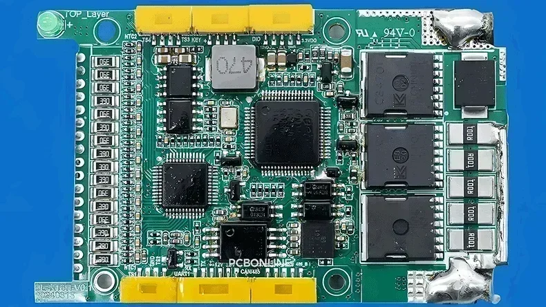
Auxiliary power units and safety systems benefit similarly. Airbag controllers and ADAS modules incorporate heavy copper for reliable power delivery amid fault conditions. These applications prioritize fault tolerance, where heavy copper reduces the risk of trace burnout under overloads.
Design Principles for Heavy Copper PCBs in Automotive
Effective design begins with current capacity calculations, guided by standards like IPC-2152 for determining trace widths based on temperature rise. Engineers must account for multilayer configurations, where inner heavy copper layers share loads with outer ones. Thermal vias filled with conductive material bridge layers for better heat transfer, a common troubleshooting fix for hotspots. Avoid narrow traces adjacent to heavy ones to prevent uneven etching during fabrication.
Material selection focuses on high Tg laminates to withstand automotive thermal profiles. Copper weight distribution varies by layer, with outer layers often heaviest for connector interfacing. Signal integrity remains key; heavy copper planes act as ground returns, but impedance control requires careful routing. Practical advice: Simulate power distribution early to identify bottlenecks before prototyping.
Via design poses challenges with heavy copper due to plating buildup. Larger annular rings and deeper plating ensure reliability, per IPC-6012 qualification specs. For automotive vibration, reinforce vias with stitching around high-current paths.
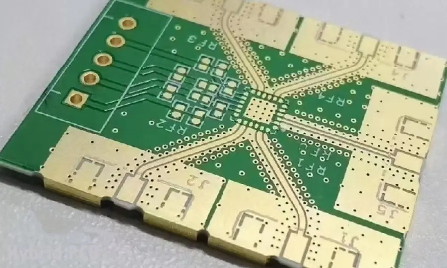
Mechanical considerations include board thickness and support structures. Heavy copper increases overall rigidity but can induce warpage if not balanced across layers. Sequential lamination builds complex stacks reliably, aiding automotive multilayer needs.
Manufacturing and Assembly Best Practices
Fabricating heavy copper PCB automotive boards involves differential etching to achieve fine features alongside thick traces. Panel plating builds copper uniformly, followed by precise tenting for protection. Troubleshooting warpage requires symmetric stackups and controlled bake cycles post-lamination.
Assembly demands low-stress soldering to avoid cracking thick copper interfaces. J-STD-001 guidelines ensure class 3 compliance for automotive reliability. Heavy copper interfaces with busbars or IGBT modules necessitate robust mechanical fastening to handle torque.
Quality control verifies copper thickness uniformity via cross-sectioning. Electrical testing under load simulates automotive currents, catching defects early.
Reliability testing mimics vehicle life: thermal shock, vibration per IEC standards, and humidity exposure. These confirm endurance in battery management system PCBs and inverters.
Troubleshooting Common Issues in Automotive Heavy Copper PCBs
Overheating tops failure modes, often from undersized traces or poor thermal paths. Solution: Recalculate per IPC-2152 and add embedded heat pipes if vias insufficient. Vibration-induced fatigue cracks vias; use filled vias and conformal coating for mitigation.
Delamination from CTE mismatch plagues high-power designs. Select low-loss dielectrics and gradient copper weights to match expansion rates. Signal noise in mixed heavy copper environments requires separated power and ground planes.
Prototyping reveals plating voids; extend electroplating cycles and inspect with X-ray.
Conclusion
Heavy copper PCBs drive automotive electronics forward, enabling PCB for electric vehicles to meet power and reliability demands. From battery management system PCB to inverters, these boards deliver practical solutions for high-current challenges. Design and manufacturing best practices, aligned with industry standards, ensure long-term performance. Engineers gain troubleshooting confidence through simulation and testing, optimizing for real-world stresses. As electrification advances, heavy copper remains pivotal for efficient, durable automotive systems.
FAQs
Q1: What defines a heavy copper PCB automotive application?
A1: Heavy copper PCB automotive refers to boards with copper layers exceeding standard thicknesses, typically 3 ounces per square foot or more, optimized for high-current handling in vehicles. These support power electronics like inverters and chargers by reducing resistance and enhancing thermal dissipation. Design per IPC-2221 ensures trace sizing matches load requirements. Troubleshooting focuses on balanced stackups to prevent warpage.
Q2: How do PCB for electric vehicles benefit from heavy copper?
A2: PCB for electric vehicles use heavy copper for superior current capacity and heat management in compact spaces. This lowers energy losses in motor drives and converters, extending range and efficiency. Vibration resistance improves reliability under road conditions. Practical integration involves thermal vias for hotspot elimination.
Q3: Why is battery management system PCB critical with heavy copper?
A3: Battery management system PCB employs heavy copper to carry high currents between cells while monitoring safely. Thick traces minimize voltage drops, aiding precise balancing and fault detection. Automotive thermal cycles demand robust plating per IPC-6012. Common fix: Enhance ground planes to reduce EMI.
Q4: What challenges arise in heavy copper automotive electronics manufacturing?
A4: Challenges include etching precision for thick copper and warpage control during lamination. Solutions involve sequential builds and symmetric designs. Assembly requires careful soldering to avoid stress cracks. Testing verifies performance under simulated vehicle loads.
References
IPC-2221B — Generic Standard on Printed Board Design. IPC, 2012
IPC-2152B — Standard for Determining Current Carrying Capacity in Printed Board Design. IPC, 2019
IPC-6012E — Qualification and Performance Specification for Rigid Printed Boards. IPC, 2017





