 ALLPCB


High-reliability printed circuit boards serve critical roles in aerospace, medical, automotive, and industrial systems where downtime or malfunction carries substantial risk. Engineers rely on systematic examination of failed assemblies to uncover the underlying issues that led to defects. This process, known as PCB failure analysis, provides the data needed to refine designs, adjust manufacturing parameters, and strengthen quality controls. When performed correctly, it directly supports efforts to prevent PCB failures in subsequent production runs. The insights gained also contribute to improving PCB reliability through failure analysis across entire product lifecycles.
What Is PCB Failure Analysis and Why It Matters
PCB failure analysis is the structured investigation of boards that have malfunctioned or degraded during testing, qualification, or field use. It combines non-destructive and destructive techniques to isolate the physical location and nature of defects. The practice matters because high-reliability applications demand consistent performance under thermal cycling, vibration, humidity, and electrical stress. Identifying PCB failure causes early reduces the chance of recurring issues and supports root cause analysis for PCB defects. Organizations that embed this discipline into their workflows see measurable gains in yield and long-term product dependability.
Common Mechanisms Leading to PCB Failures
Several engineering mechanisms repeatedly appear in failed high-reliability boards. Thermal expansion mismatch between copper, laminate, and components can generate stresses that initiate cracks in vias or delamination at interfaces. Moisture ingress followed by rapid heating during reflow or operation produces vapor pressure that separates layers, a phenomenon addressed in moisture sensitivity classifications. Electromigration occurs when high current densities and ionic contaminants drive metal atoms along conductive paths, eventually forming unintended shorts. Mechanical shock and vibration can fatigue solder joints or fracture brittle components. Each mechanism leaves characteristic signatures that trained analysts recognize through methodical inspection.
Related Reading: PCB Failure Analysis: Case Studies and Real World Examples
PCB Failure Analysis Methods
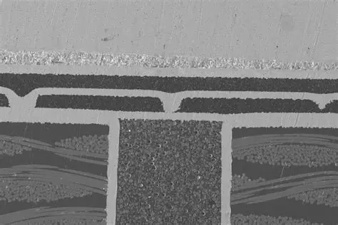
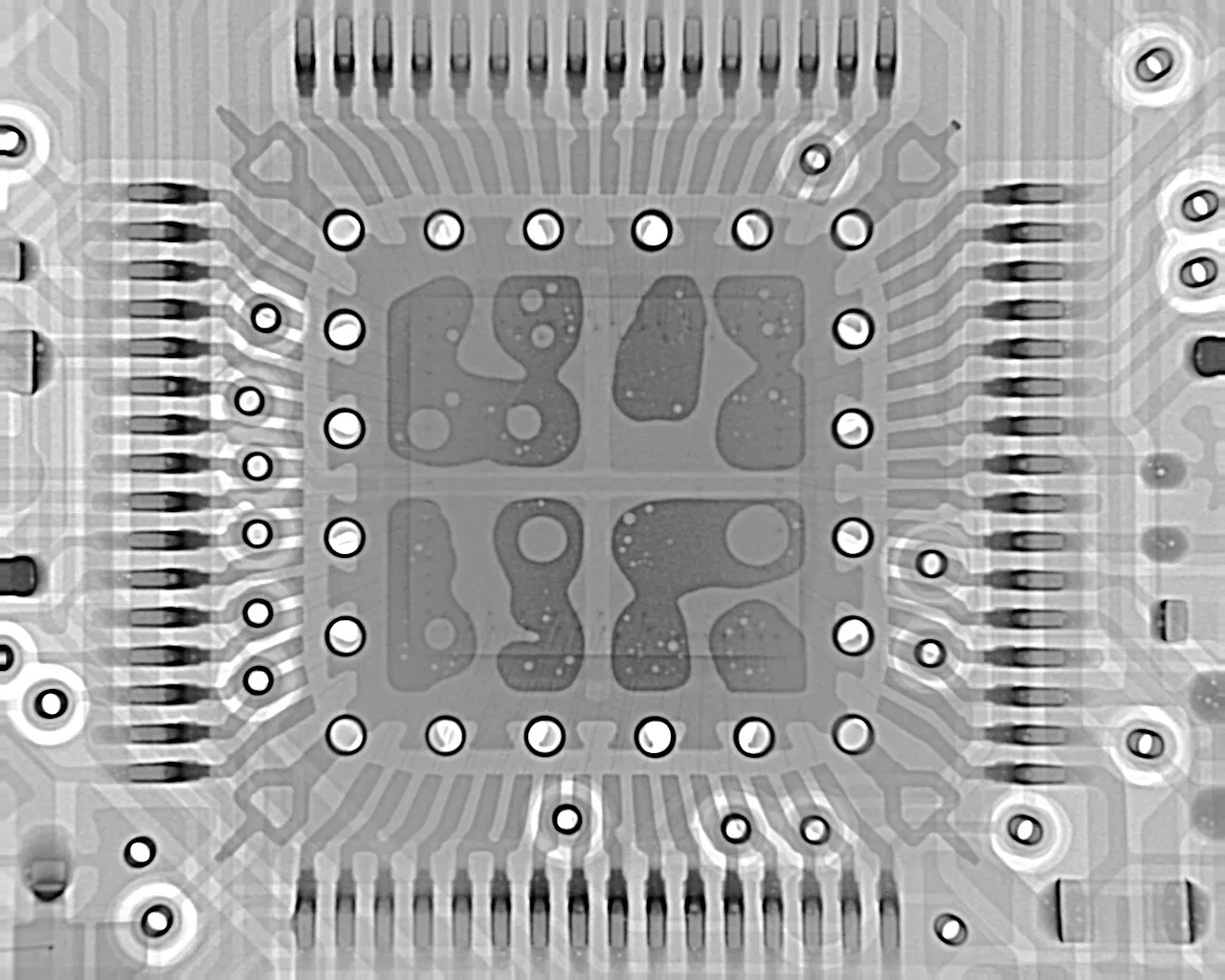
Effective PCB failure analysis methods begin with non-destructive steps before progressing to more invasive techniques. Initial visual and optical microscopy examination reveals surface anomalies such as discoloration, cracks, or foreign material. X-ray imaging then maps internal features including solder voids, misaligned vias, and hidden cracks without damaging the board. Cross-sectioning followed by polishing and microscopy exposes microstructural details such as intermetallic compound thickness or delamination planes. Electrical probing and thermal imaging locate intermittent faults or hot spots under powered conditions. When required, scanning electron microscopy with elemental analysis identifies contamination or material degradation. These layered approaches ensure comprehensive coverage while preserving evidence for root cause determination.
Related Reading: Troubleshooting PCB Failures: How Imaging Technology Aids in Root Cause Analysis
Root Cause Analysis for PCB Defects
Root cause analysis for PCB defects follows a logical sequence that links observed symptoms to originating factors. Analysts document the failure mode, map its location on the board, and correlate it with process history or environmental exposure. Fishbone diagrams or fault trees help organize potential contributors such as material lot variations, plating thickness deviations, or handling damage. Statistical review of multiple failures from the same lot often reveals patterns invisible in single incidents. Once the primary cause is isolated, corrective actions target design rules, material specifications, or process controls rather than symptoms alone. This disciplined methodology prevents recurrence and feeds directly into design-for-reliability practices.
Best Practices for Preventing PCB Failures
Preventing PCB failures starts at the design stage with appropriate material selection, via placement rules, and thermal management features. Engineers apply derating guidelines for current-carrying traces and ensure adequate spacing to reduce electromigration risk. During manufacturing, adherence to controlled processes for lamination, drilling, plating, and soldering minimizes latent defects. Incoming material inspection and in-process monitoring catch deviations before they propagate. Post-assembly testing, including thermal cycling and highly accelerated stress screening, surfaces weaknesses that would otherwise appear in the field. When failures do occur, feeding analysis results back into design and process databases closes the improvement loop and supports continuous reliability gains.
Case Insight from Structured Analysis
In one documented scenario involving multilayer boards for a vibration-intensive environment, repeated via cracking was traced to insufficient copper wrap plating thickness combined with excessive z-axis expansion of the laminate during thermal excursions. Cross-sectional analysis confirmed the plating deficiency, while material characterization verified the coefficient of thermal expansion values. Adjustments to plating process controls and selection of a lower-expansion laminate grade eliminated the failure mode in subsequent builds. The case illustrates how targeted PCB failure analysis methods translate into concrete design and process changes that improve overall reliability.
Conclusion
Systematic failure analysis transforms isolated incidents into actionable knowledge that strengthens high-reliability PCB programs. By combining established inspection techniques with rigorous root cause investigation, engineering teams identify PCB failure causes accurately and implement effective countermeasures. The result is fewer defects, higher first-pass yields, and greater confidence in long-term field performance. Organizations that treat failure analysis as an integral part of the development cycle consistently achieve better outcomes in demanding applications.
FAQs
Q1: What are the primary PCB failure analysis methods used for high-reliability boards?
A1: Primary methods include optical and scanning electron microscopy, X-ray radiography, acoustic microscopy, cross-sectioning, and electrical/thermal characterization. These techniques progress from non-destructive to destructive steps to locate and characterize defects while preserving evidence for root cause determination. The combination allows engineers to identify PCB failure causes ranging from material issues to process deviations.
Q2: How does root cause analysis for PCB defects improve product reliability?
A2: Root cause analysis systematically links observed defects to originating factors such as design choices, material properties, or manufacturing variations. By addressing the true source rather than symptoms, teams prevent recurrence across future lots. This structured approach directly supports improving PCB reliability through failure analysis and reduces costly field returns.
Q3: What steps help in preventing PCB failures during design and manufacturing?
A3: Prevention begins with material selection matched to expected thermal and mechanical loads, followed by design rules that minimize stress concentrations. Controlled processes for plating, soldering, and handling, combined with incoming inspection and stress screening, further reduce latent defects. Regular feedback from failure analysis refines these controls over time.
Q4: Why is identifying PCB failure causes important for electric engineers working on high-reliability systems?
A4: Identifying PCB failure causes enables engineers to implement targeted fixes that enhance long-term performance and safety. It provides the factual basis for design iterations and process improvements required in aerospace, medical, and automotive applications. The resulting knowledge base supports consistent compliance with performance expectations.
References
IPC-6012E — Qualification and Performance Specification for Rigid Printed Boards. IPC, 2017
IPC-A-600K — Acceptability of Printed Boards. IPC, 2020
JEDEC J-STD-020E — Moisture/Reflow Sensitivity Classification. JEDEC, 2014





