 ALLPCB


Essential PCB Design Software for Telecommunication Base Station Development
Why PCB Design Software Matters for Telecommunication Applications
Base-station PCBs must support radio-frequency transmission, power distribution, and digital control functions within compact enclosures exposed to varying environmental conditions. Telecommunication PCB layout therefore demands precise control over impedance, crosstalk, and electromagnetic compatibility. PCB design software provides the simulation and verification capabilities needed to meet these demands without repeated physical prototypes. By integrating schematic capture, layout editing, and analysis modules, the software streamlines the transition from concept to production while maintaining compliance with performance targets.
Technical Principles of Telecommunication PCB Layout
High-frequency operation in base stations introduces challenges such as transmission-line effects, skin-effect losses, and dielectric losses. Signal integrity software within PCB design platforms models these phenomena by solving Maxwell’s equations numerically or through simplified transmission-line equations. Engineers define stackup parameters, trace geometries, and material properties so that the software can calculate characteristic impedance and propagation delay. Proper modeling ensures that differential pairs maintain consistent spacing and reference planes, reducing mode conversion and radiated emissions.
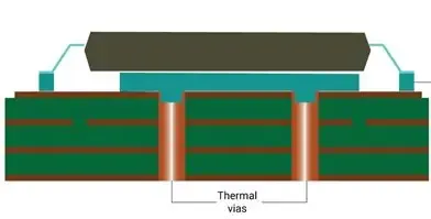
Thermal management constitutes another critical principle. Base-station amplifiers and processors generate localized heat that must be conducted away through copper planes, thermal vias, and heat sinks. PCB design software incorporates thermal simulation engines that solve heat-transfer equations across the board geometry. These simulations identify hot spots early, allowing designers to adjust copper distribution or component placement before committing to fabrication. The resulting layouts satisfy both electrical and thermal constraints simultaneously.
Best Practices in Using PCB Design Software for Base-Station Projects
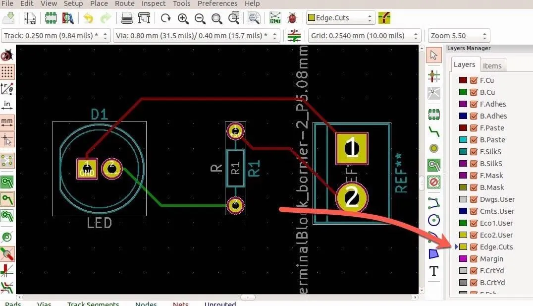
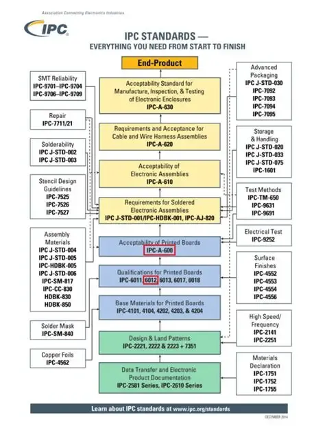
Begin with a clearly defined stackup that meets IPC-6012E requirements for rigid printed boards. The software’s layer stack manager should reflect actual dielectric thicknesses and copper weights so that impedance calculations remain accurate. Next, apply design rules that enforce minimum trace widths, clearances, and via structures consistent with the chosen fabrication process. These rules prevent violations that could compromise manufacturability or long-term reliability.
Route critical nets first, prioritizing clocks, high-speed data lines, and RF paths. Use length-matching and phase-tuning features available in most PCB design software to keep differential pairs balanced. After routing, run signal integrity simulations to verify eye diagrams and timing margins under worst-case conditions. Iterate on via placement and reference-plane continuity until margins meet system specifications.
Thermal analysis follows routing. Apply realistic power-dissipation values to components and examine temperature gradients across the board. Adjust copper pours or add thermal vias where simulations indicate excessive temperature rise. Document all changes so that the final layout file contains complete traceability for manufacturing and quality teams.
Verification and Compliance Considerations
Conclusion
PCB design software enables engineers to address the multifaceted requirements of telecommunication base-station PCBs in a structured, repeatable manner. By combining accurate stackup definition, signal-integrity analysis, and thermal simulation within a single environment, designers achieve layouts that satisfy electrical performance, thermal limits, and industry standards. Consistent application of these practices reduces prototype iterations and supports reliable field deployment of base-station equipment.
FAQs
Q1: What role does PCB design software play in telecommunication PCB layout?
A1: PCB design software integrates schematic capture, layout editing, and analysis tools that allow engineers to create multilayer boards supporting high-frequency signals and dense component placement typical of base stations. It enables precise impedance control and signal-integrity verification before fabrication.
Q2: How does signal integrity software improve telecommunication base-station designs?
A2: Signal integrity software calculates transmission-line parameters, models crosstalk, and generates eye diagrams that predict real-world performance. This capability helps engineers adjust trace geometry and reference planes to maintain signal quality across the operating frequency range of base-station equipment.
Q3: Why is thermal analysis important when using PCB design software for base stations?
A3: Base-station PCBs often dissipate significant power in amplifiers and processors. Thermal simulation within PCB design software identifies hot spots and guides the placement of copper planes and thermal vias, ensuring operating temperatures remain within component specifications and improving long-term reliability.
Q4: What standards guide the use of PCB design software for telecommunication applications?
A4: Designs typically reference IPC-6012E for rigid-board qualification and IPC-A-600K for acceptability criteria. These standards define acceptable feature sizes, plating requirements, and inspection criteria that PCB design software outputs must satisfy before release to manufacturing.
References
IPC-6012E — Qualification and Performance Specification for Rigid Printed Boards. IPC, 2017
IPC-A-600K — Acceptability of Printed Boards. IPC, 2020
ISO 9001:2015 — Quality Management Systems. ISO, 2015


