 ALLPCB


Introduction
ENEPIG stands out as a premium surface finish for printed circuit boards, offering superior performance in demanding applications. Engineers specify ENEPIG thickness IPC-4556 to ensure reliability in soldering, wire bonding, and electrical contacts. This multilayer finish consists of electroless nickel, electroless palladium, and immersion gold, each layer contributing to overall durability. Proper adherence to PCB plating standards prevents issues like corrosion and ensures long-term functionality. As electric engineers design high-frequency or high-reliability boards, grasping these specifications becomes essential for procurement and fabrication success. This article delves into the precise layer requirements and their engineering implications.
What Is ENEPIG and Why Does Layer Thickness Matter?
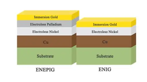
ENEPIG, or Electroless Nickel Electroless Palladium Immersion Gold, protects exposed copper traces and pads from oxidation while enabling multiple assembly processes. The nickel layer acts as a barrier and strengthens plated-through holes, the palladium layer shields the nickel during gold deposition and supports wire bonding, and the gold layer provides solderability and corrosion resistance. Deviations in ENEPIG nickel thickness, ENEPIG palladium thickness, or ENEPIG gold thickness can lead to failures such as poor solder joints or bond lifts.
Layer thicknesses directly impact electrical performance, thermal cycling reliability, and shelf life. For instance, insufficient nickel compromises structural integrity, while excessive gold risks diffusion into underlying layers. IPC-4556 establishes ENEPIG thickness IPC-4556 requirements to balance cost, performance, and manufacturability across rigid and flexible boards. Engineers must consider these PCB plating standards during design reviews to avoid field failures in automotive, aerospace, or telecom applications. Uniformity across panels ensures consistent assembly yields.
The Technical Principles of ENEPIG Layer Thicknesses
IPC-4556 defines electroless nickel thickness as 3.0 to 6.0 micrometers, measured in microinches as 118.1 to 236.2 on a nominal 1.5 mm by 1.5 mm pad or equivalent area. This range provides adequate barrier protection against copper diffusion during soldering and reflow, while supporting mechanical stress in plated-through holes. Phosphorus content in the nickel, typically mid to high at 8 to 10 weight percent, enhances corrosion resistance without brittleness. Thinner nickel suits fine-pitch designs, but falls below 3.0 micrometers increase risks of hyper-corrosion under thermal stress.
Electroless palladium thickness ranges from 0.05 to 0.15 micrometers, or 2.0 to 12.0 microinches, serving as a critical intermediary. Palladium prevents the immersion gold reaction from corroding the nickel, a common ENIG failure mode known as black pad. Its electroless deposition ensures conformal coverage on high-aspect-ratio features. Adequate thickness enables aluminum or gold wire bonding with pull strengths exceeding industry benchmarks, vital for flip-chip or hybrid assemblies.
Immersion gold thickness specifies a minimum of 0.030 micrometers or 1.2 microinches at minus four sigma from the process mean, with a maximum of 0.070 micrometers or 2.8 microinches per the 2015 amendment. This thin layer oxidizes minimally, preserving solder wettability over 12 months shelf life. Excess gold promotes intermetallic compound formation, degrading joint reliability during multiple reflows. All measurements account for process variation using X-ray fluorescence at plus or minus four sigma, ensuring statistical process control.
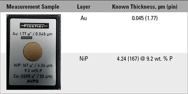
These specifications apply uniformly, with tolerances tightened in IPC-4556A for enhanced precision. Engineers verify compliance through cross-section SEM analysis or non-destructive methods during qualification.
Best Practices for Achieving IPC-4556 Compliant ENEPIG
Fabrication begins with clean copper activation to promote uniform electroless nickel deposition. Process parameters like bath pH, temperature, and load factor control ENEPIG nickel thickness uniformity across panels. Rinsing between layers minimizes drag-out, preventing defects like palladium nodules.
For ENEPIG palladium thickness, select baths with low phosphorus palladium precursors for stability and adhesion. Monitor deposition rate to stay within 0.05 to 0.15 micrometers, adjusting stabilizers for high-volume production. Gold immersion follows immediately, with dwell times calibrated to hit the 0.03 to 0.07 micrometer target without overplating.
Quality control integrates IPC-6012 qualification testing alongside thickness verification. Use coupon panels matching production panels for representative sampling. Statistical process control charts track sigma levels, rejecting lots outside four sigma limits.
Procurement specs should explicitly call out ENEPIG thickness IPC-4556, including measurement pad size and sigma criteria. Collaborate with fabricators on phosphorus analysis via EDS to correlate with thickness accuracy.
Troubleshooting Common ENEPIG Thickness Issues
Non-uniform ENEPIG gold thickness often stems from contaminated immersion baths, leading to patchy solderability. Inspect via optical microscopy and reflow test coupons per J-STD-001. Thin spots below 0.03 micrometers accelerate oxidation, while thick areas signal copper or nickel drag-in.
ENEPIG nickel thickness below spec arises from bath exhaustion or poor activation, weakening PTH barrels. Cross-section analysis reveals voids or thinning at vias. Adjust hypophosphite concentration and replenishment rates for recovery.
Palladium layer inconsistencies manifest as nickel corrosion pits under SEM, mimicking ENIG black pad. Verify ENEPIG palladium thickness exceeds 0.05 micrometers and phosphorus content. Rework involves stripping and replating, but prevention through bath monitoring proves more efficient.
Field failures link to thermal mismatch; thicker nickel buffers CTE differences in multilayer stacks. Reference IPC-A-600 acceptability criteria during incoming inspection.
Conclusion
Mastering ENEPIG layer thicknesses per IPC-4556 ensures robust PCB performance across assembly challenges. The 3 to 6 micrometer nickel, 0.05 to 0.15 micrometer palladium, and 0.03 to 0.07 micrometer gold balance protection, bondability, and cost. Electric engineers benefit from specifying these PCB plating standards upfront, integrating process controls for yield optimization. Adhering to measurement protocols at four sigma mitigates variability, extending reliability in high-stakes designs. Prioritize standard compliance to future-proof assemblies against evolving demands.
FAQs
Q1: What is the ENEPIG nickel thickness specified in IPC-4556?
A1: IPC-4556 requires electroless nickel thickness of 3.0 to 6.0 micrometers, or 118.1 to 236.2 microinches, on a 1.5 mm by 1.5 mm pad at plus or minus four sigma. This range supports PTH integrity and solder joint strength. Engineers specify mid-range for fine-pitch boards to avoid brittleness.
Q2: How does ENEPIG palladium thickness impact wire bonding?
A2: ENEPIG palladium thickness of 0.05 to 0.15 micrometers prevents nickel corrosion and enables high pull strength bonds. Thinner layers risk black pad-like defects, while optimal thickness ensures aluminum or gold wire compatibility per IPC standards. Verify via bond testing during qualification.
Q3: What are the ENEPIG gold thickness limits under IPC-4556?
A3: Immersion gold thickness minimum is 0.030 micrometers at minus four sigma, maximum 0.070 micrometers to curb diffusion. This preserves solder wettability without excess intermetallics. Non-destructive XRF confirms compliance on production panels.
Q4: Why follow PCB plating standards like IPC-4556 for ENEPIG?
A4: These standards define layer tolerances for soldering, bonding, and contact reliability, reducing defects like corrosion. They incorporate statistical controls for process capability. Electric engineers use them to align design with fabrication, ensuring consistent performance.
References
IPC-4556A — Specification for Electroless Nickel/Electroless Palladium/Immersion Gold (ENEPIG) Plating for Printed Boards. IPC, 2025
IPC-6012E — Qualification and Performance Specification for Rigid Printed Boards. IPC, 2017
IPC-A-600K — Acceptability of Printed Boards. IPC, 2020





