 ALLPCB


Introduction
Flexible printed circuit boards, or flex PCBs, enable compact electronics in applications where space constraints and mechanical movement are critical, such as wearables, medical devices, and aerospace systems. Altium Designer provides comprehensive tools for designing these circuits, including support for both pure flex and rigid-flex configurations. This Altium Designer flexible PCB tutorial guides electrical engineers through the process, emphasizing the Layer Stack Manager, design rules, and routing techniques. By following these steps, designers can create reliable flex circuits that meet performance demands while adhering to manufacturing constraints. The tutorial focuses on practical implementation within Altium's unified environment.
What Are Flexible PCBs and Why Do They Matter?
Flexible PCBs consist of thin copper layers laminated on flexible substrates like polyimide, allowing bending and folding without compromising electrical integrity. Unlike rigid boards, flex circuits reduce weight, eliminate connectors, and fit into irregular shapes, making them essential for dynamic environments. Rigid-flex designs combine rigid sections for components with flex tails for interconnections, enhancing reliability in high-vibration settings. Industry relevance grows with miniaturization trends, where traditional wiring fails due to bulk and fatigue. Designing flex circuits in Altium ensures precise control over stackups and bends, minimizing risks like trace cracking. Proper design aligns with standards such as IPC-2223, which outlines sectional requirements for flexible and rigid-flex boards.
Technical Principles of Flex PCB Design
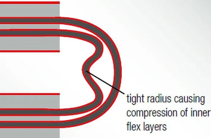
Flex PCB performance hinges on material selection and bend geometry. Substrates must withstand repeated flexing, with copper foils chosen for ductility to prevent cracking under strain. Bend radius is a key parameter, determined by layer count, copper type, and application type, static or dynamic. For instance, minimum radii range from 5:1 for single-layer static bends to 40:1 for multilayer dynamic ones, preventing delamination or trace fractures. Layer staggering offsets traces between layers to distribute stress evenly, avoiding I-beaming effects. Coverlays protect traces while maintaining flexibility, and hatched planes preserve pliability over solid fills. These principles ensure longevity, with IPC-6013 specifying qualification tests for flex and rigid-flex boards.
Step-by-Step Guide to Designing Flex PCBs in Altium Designer
Step 1: Project Setup and Enabling Rigid-Flex Features
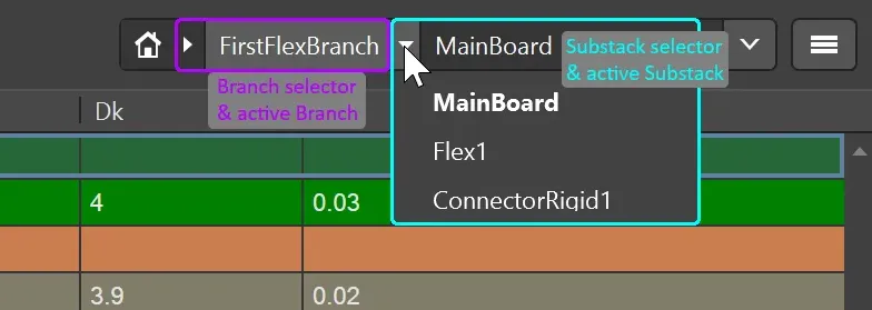
Start by creating a new PCB project in Altium Designer and importing or drawing the schematic. Compile the schematic, then transfer to PCB via Design > Import Changes. To enable flex support, open the Layer Stack Manager with Design > Layer Stack Manager. Select Tools > Features > Rigid-Flex (Advanced) for complex designs supporting overlapping regions and substacks, or Rigid-Flex for simpler ones. Advanced mode is recommended for most Altium rigid-flex designs, offering visual substack editing. Confirm the mode in the Active Bar while in Board Planning Mode (shortcut: 1).
Step 2: Configuring the Layer Stack Manager for Flex
In the Layer Stack Manager's Board tab (advanced mode), define substacks representing rigid and flex sections. Add a flex substack by Shift-clicking layers and using the Add Substack button, then enable Is Flex in the Properties panel. Select polyimide-like materials for dielectrics via the Material dialog, setting thickness, Dk, and Df values appropriate for flex. Add coverlay layers only in flex substacks, as they replace solder mask. Configure impedance profiles in the Impedance tab for controlled traces, specifying width and gap for target values. Enable Stack Symmetry if needed for balanced structures. Save changes to update the PCB editor.
Step 3: Defining Board Regions and Assigning Substacks
Switch to Board Planning Mode (View > Board Planning Mode). Place board regions with Place > Board Region, drawing polygons for rigid and flex areas. For rigid-flex, create overlapping regions where flex tails extend from rigid bodies. Assign substacks via the PCB panel in Layer Stack Regions mode or Properties panel, naming regions for clarity. Lock the 3D position of a rigid region as Z=0 reference. Slice regions if needed with Design > Slice Board Region, choosing corner modes like arcs for smooth transitions. This setup, central to Altium rigid-flex design, prepares the board for folding visualization.
Step 4: Setting Altium Flex PCB Design Rules
Access design rules via Design > Rules. Create rules for flex regions targeting Minimum Width, Clearance, and Routing Corner Style, prioritizing curved arcs over 90-degree angles to reduce stress. Set board edge clearances higher near flex interfaces, such as 20 mils for vias. Restrict vias and components to rigid areas using Rooms or Clearance rules. For pads, enable teardrops and fillets to anchor against peel. Define polygon connection styles as hatched for planes in flex substacks. Run Design Rule Check (DRC) early to validate Altium flex PCB design rules compliance. These rules prevent common failures like trace fatigue.
Step 5: Component Placement and Altium Routing for Flex Circuits
Place components on rigid regions first, using interactive drag for alignment. Switch to 2D Layout Mode for standard placement. For routing, use interactive routing (Route > Interactive Routing) with arc corner modes (Shift+Spacebar). In flex areas, widen traces gradually and stagger them across layers. Avoid vias in dynamic bend zones, opting for supported vias in stiffeners if essential. Route power planes as hatched fills. Maintain service loops, extra length for assembly tolerances. Verify impedance with the Impedance Calculator during routing.
Step 6: Defining Bending Lines and 3D Visualization
In Board Planning Mode, place bending lines via Place > Define Bending Line across flex regions. Edit properties in the Properties panel: set Bend Angle, Radius (per IPC-2223 guidelines), and Fold Index for sequence. Lines auto-extend to region edges. Use the Fold State slider to preview bends in 3D (View > 3D Layout Mode). Adjust for realistic folding, ensuring no inter-layer shorts. This feature visualizes stresses early.
Step 7: Finalization, DRC, and Output Generation
Run full DRC and compile changes. Place a Layer Stack Table (Place > Layer Stack Table) for documentation. Generate fabrication outputs via File > Fabrication Outputs, including stackup diagrams and drill files noting flex regions. Review in 3D for mechanical fit.
Best Practices for Reliable Flex Designs
Always consult fabricators for material specifics, as flex requires adhesiveless laminates for dynamic use. Minimize layer count in high-flex areas to ease bending. Use RA copper for ductility over ED types. Document bend directions and radii in notes. Test prototypes per IPC-6013 for qualification. These practices extend cycle life significantly.
Conclusion
Mastering flexible PCB design in Altium Designer involves precise layer stack management, region definition, and rule-driven routing. This Altium Designer flexible PCB tutorial equips engineers to produce manufacturable designs efficiently. Key takeaways include leveraging advanced rigid-flex mode, curved routing, and standards compliance for durability. With these steps, teams can innovate in compact, reliable electronics.
FAQs
Q1: How does the Altium layer stack manager support rigid-flex design?
A1: The Layer Stack Manager in advanced mode allows defining multiple substacks for rigid and flex regions, with visual Board tab editing. Enable Is Flex for coverlay and polyimide materials, assign to regions via PCB panel. Impedance and via tabs ensure signal integrity. This unifies stackup across the design, simplifying Altium rigid-flex design.
Q2: What are essential Altium flex PCB design rules for routing?
A2: Set rules for curved corners, increased widths in bends, and hatched planes to minimize stress. Restrict vias to rigid zones with Clearance rules, add teardrops to pads. Prioritize arc modes in interactive routing for smooth traces. These Altium flex PCB design rules prevent fatigue in dynamic applications.
Q3: How to route traces effectively for flex circuits in Altium?
A3: Use interactive routing with arc corners, stagger layers to avoid overlap, and widen in bend zones. Apply design rules for minimum radius adherence. Preview in 3D after bending lines. Altium routing for flex circuits excels with real-time DRC feedback.
Q4: What standards guide designing flex circuits in Altium?
A4: IPC-2223 provides bend radius and layout guidelines, while IPC-6013 ensures performance qualification. Incorporate these in rules and stackups for compliance. Altium tools facilitate adherence through documentation features.
References
IPC-2223E - Sectional Design Standard for Flexible/Rigid-Flex Printed Boards. IPC, 2020
IPC-6013D - Qualification and Performance Specification for Flexible and Rigid-Flex Printed Boards. IPC, 2016


