 ALLPCB


Introduction
Blind via routing represents a critical advancement in PCB routing techniques for modern high-density designs. These vias enable engineers to connect surface layers to internal layers without penetrating the entire board stackup, freeing up valuable routing space on unused layers. As electronic devices demand smaller footprints and higher performance, blind via routing becomes essential for efficient layout and signal management. This approach minimizes via stubs that can degrade signal integrity in high-speed applications. By mastering blind via routing, designers achieve denser interconnects while adhering to manufacturability constraints. This article outlines structured best practices drawn from engineering principles to optimize PCB layouts.
What Are Blind Vias and Why Do They Matter in PCB Routing?
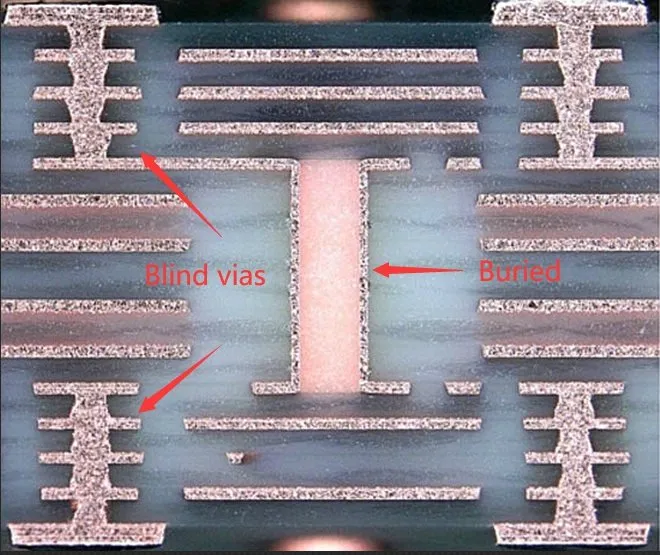
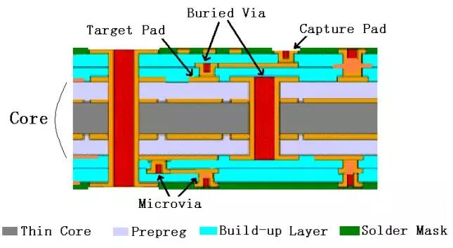
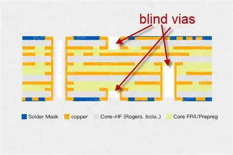
Blind vias connect an outer layer, such as the top or bottom, to one or more inner layers without extending through the full board thickness. Unlike through vias, which traverse all layers and obstruct inner routing channels, blind vias remain invisible from the opposite side. They differ from buried vias, which link only internal layers, by providing access from the surface for component connections. In PCB routing techniques, blind vias support high-density interconnects by allowing traces on inner layers to route freely beneath surface pads.
The relevance of blind via routing grows with the push for compact electronics, where board real estate limits traditional through-via usage. They reduce layer count requirements, lowering material costs and board weight in applications like smartphones and servers. For signal management, blind vias shorten return paths, reducing inductance and improving impedance control compared to longer through vias. Efficient layout becomes possible as these vias eliminate unnecessary drill depths, enhancing thermal dissipation by preserving copper planes. Overall, blind vias enable design tips that balance density, performance, and reliability in complex multilayer boards.
Technical Principles Behind Blind Via Routing
Blind vias rely on precise fabrication processes to ensure reliability. Manufacturers typically use sequential lamination, where core sections are built incrementally, drilled, plated, and laminated together. Laser drilling suits smaller diameters under 150 microns, while mechanical drilling handles larger ones up to 250 microns. Plating follows to fill the barrel with copper, achieving uniform conductivity across the via structure.
Key engineering parameters govern blind via performance. The aspect ratio, defined as depth to diameter, must stay below 1:1, ideally 0.8:1, to prevent plating voids from poor electrolyte penetration. IPC-2221 provides guidelines for via dimensions and spacing in rigid board designs, emphasizing clearance rules to avoid shorts. Signal propagation through blind vias demands controlled impedance, as transitions affect characteristic impedance by up to 20 percent without optimization.
Layer stackup planning dictates blind via feasibility. Engineers specify via start and end layers during design, ensuring alignment with core thicknesses. Cross-section analysis reveals potential issues like misalignment from lamination shrinkage. Adhering to these principles supports robust signal management in high-frequency environments.
Best Practices for Blind Via Routing in PCB Layout
Stackup and Via Planning
Begin with a thorough stackup definition to integrate blind vias effectively. Identify layers needing interconnection and allocate blind vias to span only required depths, preserving routing channels elsewhere. Simulate the stackup for warpage and CTE mismatch, as blind vias concentrate stresses at edges. Limit blind via usage to 20 percent of total vias initially to control costs, scaling based on density needs.
Incorporate design rules early: set minimum via diameter at 100 microns for laser types, with pads 300 microns larger per industry norms. Space adjacent vias at least 0.2 mm edge-to-edge to facilitate drilling accuracy. Plan via tents or fills for exposed ends to protect against solder wicking during assembly.
Optimal Placement Strategies
Position blind vias close to components for shortest fanout traces, minimizing parasitic inductance. Avoid placing them in high-current paths unless filled, as unfilled barrels limit current capacity to 1 A per 100 microns diameter. In BGA areas, use blind vias under balls to escape signals directly to inner planes, optimizing efficient layout.
For signal management, cluster blind vias in arrays with staggered patterns to equalize drill depths across panels. Reserve outer layers for high-speed signals, transitioning via blind vias to ground planes for return path integrity. Maintain symmetry in differential pairs by mirroring via placements, preventing skew.
Routing Techniques Around Blind Vias
Employ curved trace entries into blind via pads to reduce reflections, avoiding 90-degree bends within 3 times the trace width. Length-match routes using blind vias by adjusting serpentine patterns on inner layers. For multilayer routing, fanout blind vias perpendicular to the pad edge, ensuring annular ring exposure for inspection.
IPC-6012E outlines performance specs for rigid boards with blind vias, stressing annular ring integrity above 50 microns. Integrate stitching vias nearby for power integrity, spaced every 5 mm along planes. These PCB routing techniques enhance signal management without excessive layer transitions.
Signal Integrity Considerations
Blind vias excel in high-speed designs by eliminating stubs longer than 0.25 mm, which cause resonance above 5 GHz. Model via transitions with 3D field solvers to verify impedance at 50 ohms single-ended or 100 ohms differential. Use backdrilling as an alternative for deeper connections if blind via costs escalate.
Minimize via count in critical nets by combining blind and buried vias in hybrid stackups. Enforce ground via fencing around high-speed blind vias to shield crosstalk, maintaining 3H spacing where H is trace height. These design tips ensure robust performance under IPC guidelines.
Common Challenges and Troubleshooting in Blind Via Routing
Fabrication yields drop with blind vias due to depth control errors in mechanical drilling. Verify drill depths via X-ray during prototyping to catch offsets exceeding 50 microns. Plating nonuniformity arises from high aspect ratios, resolved by pulse electroplating sequences.
Reliability issues like cracking emerge from thermal cycling; IPC-6016 specifies HDI quals with 1000 cycles at -40 to 125 C. Troubleshoot opens by sectioning suspect vias, revealing barrel pull-away. Mitigate by oversizing pads and selecting low-loss dielectrics.
Design iterations often reveal routing congestion; refactor by promoting signals to buried vias where possible. These structured approaches maintain efficient layout despite challenges.
Conclusion
Blind via routing transforms PCB routing techniques for dense, high-performance boards. By prioritizing stackup planning, precise placement, and signal-focused routing, engineers achieve superior efficient layout and signal management. Adhering to aspect ratios under 1:1 and clearances above 0.2 mm ensures manufacturability. These best practices, grounded in standards like IPC-2221 and IPC-6012E, deliver reliable designs. Implement them iteratively with simulations for optimal results. Mastering blind via routing elevates design capabilities in demanding applications.
FAQs
Q1: What aspect ratio should engineers target for blind via routing in PCB designs?
A1: Target an aspect ratio below 1:1, ideally 0.8:1, for reliable plating and void-free barrels in blind via routing. This rule supports manufacturability in multilayer stackups, preventing electrolyte starvation during fabrication. Deeper vias risk reliability failures under thermal stress. Always verify with stackup simulations for precise depth control. These PCB routing techniques enhance signal management without added layers.
Q2: How do blind vias improve signal integrity compared to through vias?
A2: Blind vias shorten interconnect paths and eliminate long stubs, reducing inductance and reflections in high-speed signals. They preserve inner layer routing space, enabling better plane referencing for return currents. In efficient layout, this minimizes crosstalk and maintains impedance control. Designers apply these design tips to achieve cleaner eye diagrams above 10 Gbps. Overall, blind via routing outperforms through vias in dense boards.
Q3: What are key spacing rules for blind via placement in PCB routing techniques?
A3: Maintain at least 0.2 mm edge-to-edge spacing between blind vias to ensure drilling precision and avoid shorts. Pad diameters should exceed via holes by 300 microns post-plating for annular ring strength. Cluster vias thoughtfully to balance density and manufacturability. These practices support signal management in HDI layouts. Consult stackup for panel-level uniformity.
Q4: When should engineers choose blind vias over buried vias for efficient layout?
A4: Opt for blind vias when surface-to-inner connections are needed, as they access outer layers directly unlike buried types. Use them for BGA escapes in space-constrained designs to free inner routing. Blind vias suit HDI with fewer lamination steps than stacked buried configurations. Balance with cost, favoring blind for prototypes. This design tip optimizes PCB routing techniques for performance.


