 ALLPCB


Introduction
Flexible printed circuit boards, or flex PCBs, offer unique advantages in compact, dynamic applications such as wearables, medical devices, and automotive systems. Their ability to bend and conform to irregular shapes makes them indispensable for modern electronics where space constraints and mechanical movement are factors. However, these benefits come with design challenges that can lead to failures like flexible PCB cracking, delamination, and trace damage. Electrical engineers must understand these issues to ensure long-term reliability and performance. Troubleshooting these problems requires a systematic approach rooted in material properties, design rules, and manufacturing processes. This guide provides logical, structured explanations and practical solutions to common flexible PCB design problems, helping engineers optimize their designs from the outset.

Why Flexible PCBs Fail: Key Mechanisms and Industry Relevance
Flexible PCBs consist of thin copper traces laminated onto polyimide or polyester substrates, which allow repeated bending without rigid board limitations. Failures often stem from mechanical stress, thermal expansion mismatches, or environmental exposure during design, manufacturing, or use. Flexible PCB reliability issues arise when these stresses exceed material limits, leading to cracks, delamination, or trace fractures that compromise electrical continuity. In high-stakes applications, such failures can result in system downtime or safety risks, underscoring the need for proactive design strategies. Engineers must consider the interplay of substrate ductility, copper ductility, and adhesive integrity to predict and prevent these vulnerabilities. Adhering to established standards ensures designs withstand real-world conditions.
Flexible PCB Cracking: Root Causes and Detection
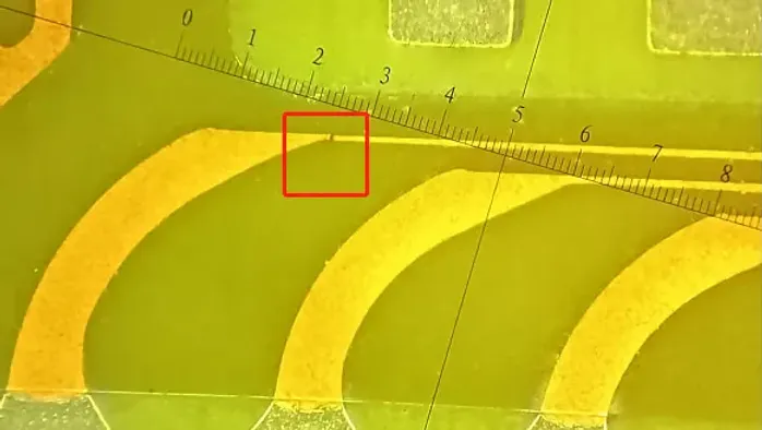
Flexible PCB cracking typically occurs in the copper traces or coverlay during repeated bending or tight radius folds. The primary cause is insufficient bend radius relative to the circuit's thickness, concentrating strain at the outer fibers of the bend. Poor trace routing, such as sharp corners or excessive trace density in flex zones, exacerbates this by creating stress risers. Manufacturing variations, like uneven lamination or copper grain inconsistencies, can also initiate micro-cracks that propagate under cyclic loading. Engineers can detect cracking through visual inspection, electrical continuity testing, or bend cycle simulations. Early identification prevents field failures by allowing redesign iterations.
IPC-2223 provides design guidelines for bend radii and trace layouts to minimize cracking risks in flexible sections. Following these rules, engineers should aim for smooth, teardrop-shaped transitions at trace bends and avoid stacking traces in high-flex areas. Substrate selection plays a role too, as polyimide offers better crack resistance than polyester in dynamic applications. Testing protocols involve controlled bend cycles to simulate operational life, revealing weaknesses before production.
Flexible PCB Delamination: Material and Process Factors
Delamination in flexible PCBs manifests as separation between copper foil, adhesive, and substrate layers, often triggered by moisture absorption followed by high-temperature exposure. During assembly reflow soldering, trapped moisture vaporizes, creating internal pressure that delaminates layers. Design flaws like inadequate coverlay adhesion or thin adhesive layers contribute, especially in multi-layer flex constructions. Environmental factors, such as humidity during storage, accelerate this failure mode. Cross-section microscopy confirms delamination by showing voids or gaps at interfaces. Addressing it early maintains interlayer integrity crucial for signal integrity.
In humid environments, pre-baking boards per industry practices removes absorbed moisture before processing. Engineers should specify adhesives with high peel strength and ensure uniform lamination pressure during fabrication. IPC-6013 outlines qualification tests, including thermal shock and humidity exposure, to verify delamination resistance. Layer stackup optimization, with balanced copper weights, further reduces differential expansion stresses.
Flexible PCB Trace Damage: Stress Analysis and Prevention
Trace damage in flex PCBs often appears as fractures or necking in copper conductors, particularly in dynamic bend zones. Excessive strain from tight bends or vibration causes plastic deformation beyond the copper's elongation limit, leading to open circuits. Improper patterning, like narrow traces or right-angle turns, localizes stress and promotes fatigue. Manufacturing defects, such as over-etching or plating voids, weaken traces predisposing them to damage. Continuity probes and high-magnification imaging diagnose the extent of damage. Proactive design mitigates these risks through strain distribution.
Engineers employ finite element analysis to model strain during bending, ensuring traces remain below yield points. Widening traces in flex areas and using curved routing paths disperses stress evenly. Stiffeners at transition zones limit flex extent, protecting traces. Adopting IPC-2223 bend zone classifications guides static versus dynamic flex designs appropriately.
Flexible PCB Reliability Issues: Holistic Testing Approaches
Flexible PCB reliability issues encompass a range of failures under combined thermal, mechanical, and electrical stresses. Thermal cycling induces fatigue from coefficient of thermal expansion mismatches between copper and substrate. Vibration or shock in applications like sensors amplifies mechanical wear, accelerating cracking or delamination. Long-term reliability demands accelerated life testing to predict field performance. Engineers must integrate reliability modeling early, considering duty cycles and environmental profiles. Comprehensive qualification verifies design robustness.
Standard tests include temperature-humidity-bias for corrosion resistance and mechanical shock for bond strength. Data logging during bend cycling quantifies cycles to failure, informing design margins. Material datasheets provide baseline ductility and adhesion values for simulations. Collaborative reviews between design and manufacturing teams catch potential issues upstream.
Flexible PCB Manufacturing Defects: Inspection and Control
Flexible PCB manufacturing defects often trace back to process variations like inconsistent lamination, coverlay misalignment, or contamination. These lead to voids, wrinkles, or weak bonds that manifest as cracking or delamination post-assembly. Poor handling introduces scratches or fingerprints, compromising surface integrity. Dimensional instability from improper curing causes warpage, stressing traces. Automated optical inspection and X-ray reveal subsurface defects efficiently. Quality control at each step prevents downstream failures.
SPC charts monitor key parameters like peel strength and thickness uniformity. Cleanroom protocols minimize contamination risks. Final electrical testing under flex conditions validates manufacturing quality.
Repairing Flexible PCBs: When and How to Intervene
Repairing flexible PCBs is challenging due to their thin, delicate nature, but feasible for prototypes or low-volume fixes. Flexible PCB trace damage from cracking requires precise techniques like conductive epoxy bridging or laser soldering. Delamination spots may need localized re-lamination with compatible adhesives after cleaning. Stiffeners or patches reinforce weak bend zones without altering functionality. Always assess repair impact on overall reliability through post-repair testing. Prevention remains superior to repair in production designs.
For trace repairs, align replacement conductors carefully and insulate with flexible coverlay. Avoid heat-intensive methods that risk further delamination. Document repairs for traceability in engineering records.
Best Practices for Designing Reliable Flexible PCBs
Successful flex PCB designs prioritize bend zone definition, material matching, and margin stacking. Classify regions as static, semi-dynamic, or dynamic per guidelines to tailor trace widths and radii. Simulate mechanical and thermal loads iteratively. Collaborate with fabricators for DFM feedback on stackups. Prototype testing under real conditions validates assumptions. These practices minimize flexible PCB reliability issues comprehensively.
Conclusion
Troubleshooting flexible PCB design problems demands a deep understanding of mechanical behaviors and material limits. By addressing flexible PCB cracking, delamination, trace damage, reliability issues, manufacturing defects, and repair needs systematically, engineers can deliver durable solutions. Standards like IPC-6013 and IPC-2223 provide the framework for qualification and design excellence. Implementing best practices ensures flex PCBs meet demanding applications reliably. Proactive design trumps reactive fixes, fostering innovation in compact electronics.
FAQs
Q1: What causes flexible PCB cracking and how can it be prevented?
A1: Flexible PCB cracking results from tight bend radii, sharp trace corners, or repeated flexing beyond material limits. Prevention involves specifying minimum bend radii per design standards, using curved trace routing, and avoiding trace stacking in flex zones. Testing with controlled bend cycles verifies durability. This approach maintains trace integrity over operational life.
Q2: How do you identify and fix flexible PCB delamination?
A2: Delamination appears as layer separation, often from moisture during reflow, detected via cross-section analysis or ultrasound. Fix by baking to remove moisture, using high-adhesion materials, and ensuring uniform lamination. Qualification tests confirm resistance. Proper handling prevents recurrence.
Q3: What are common flexible PCB trace damage issues in design?
A3: Trace damage stems from strain concentration in bends, narrow traces, or vibration. Mitigate with wider traces in flex areas, teardrop pads, and stiffeners. Simulate stress distribution for optimization. This enhances flexible PCB reliability issues resolution.
Q4: Can flexible PCBs be repaired effectively after manufacturing defects?
A4: Yes, minor defects like trace breaks use conductive inks or epoxy, while delamination needs adhesive reapplication. Test repairs rigorously for reliability. However, redesign prevents flexible PCB manufacturing defects long-term.


