 ALLPCB


Introduction
In modern high-power electronics, effective thermal management and high-current PCB design have become critical challenges for electric engineers. Components such as power amplifiers, LEDs, and processors generate substantial heat that can compromise reliability and performance if not dissipated efficiently. Advanced PCB vias, particularly via-in-pad configurations, offer solutions by integrating thermal pathways directly into component footprints. Among these, copper coin vias stand out for their superior heat conduction capabilities in demanding applications. This article explores copper coin vias and other specialty PCB vias, providing structured insights into their principles, implementation, and best practices. Engineers can leverage these techniques to enhance thermal management while maintaining compact layouts.
Understanding Via-in-Pad Technology and Its Importance
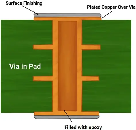
Via-in-pad technology positions vias directly within the solder pads of surface-mount components, maximizing routing density and minimizing signal path lengths. This approach contrasts with traditional dog-bone or fanout vias, which consume extra board space and introduce inductance. In high-current PCB design, via-in-pad enables better electrical connectivity and heat transfer from components to inner planes or external sinks. Its relevance grows in multilayer boards where space constraints and power densities exceed standard capabilities. For thermal management, these vias act as conduits, spreading heat laterally and vertically through the stackup. Electric engineers appreciate this for applications requiring high reliability under thermal stress.
The evolution of advanced PCB vias addresses limitations of standard through-hole or blind vias, such as solder wicking and impedance mismatches. Copper coin vias represent a pinnacle innovation, embedding solid copper elements to achieve exceptional thermal conductivity. Other specialty PCB vias, like filled and capped variants, support high-density interconnects (HDI) while aiding dissipation. These techniques matter because they prevent hotspots, reduce junction temperatures, and extend component lifespans in power electronics. Compliance with standards like IPC-6012 ensures performance in rigid printed boards. Without such advancements, high-current designs risk failure modes like delamination or electromigration.
Technical Principles of Copper Coin Vias
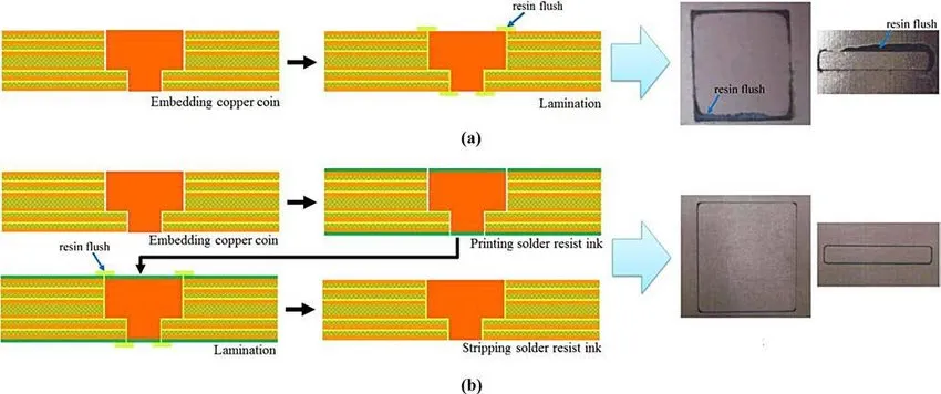
Copper coin vias involve embedding cylindrical or rectangular solid copper inserts into the PCB core, typically beneath heat-generating components. These coins provide a direct, low-resistance thermal path due to copper's high thermal conductivity, far surpassing that of plated vias or FR4 substrate. The principle relies on mechanical interlocking or adhesive bonding to integrate the coin during lamination, ensuring coplanarity with surface layers. Heat from the component flows through the coin to lower layers or a backside heatsink, bypassing less efficient vias arrays. This technique excels in thermal management for high-power densities where traditional methods fall short.
Manufacturing begins with precision milling of cavities in the core layers to match coin dimensions, followed by insertion and lamination under controlled pressure. Surface planarization via grinding or polishing maintains flatness for soldering. Variations include press-fit coins for mechanical stability or laminated coins bonded with conductive films. Engineers must consider coefficient of thermal expansion (CTE) mismatch between copper and laminate to minimize warpage. IPC-4761 guidelines for via protection influence related filled via processes, ensuring robustness in embedded structures. Overall, copper coin vias transform PCBs into active heat spreaders.
Other Innovations in Advanced PCB Vias
Beyond copper coins, filled vias represent a key specialty PCB via for via-in-pad applications. Conductive or non-conductive epoxy fills the via barrel after plating, eliminating air gaps and solder voids during reflow. This enhances thermal transfer in arrays under power devices and supports planar surfaces for BGA components. Capped vias, or via-in-pad plated over (VIPPO), add a copper cover over the fill, creating seamless pads indistinguishable from solid copper. These innovations improve signal integrity by reducing stubs and reflections in high-speed designs.
Blind and buried microvias extend via-in-pad capabilities in HDI boards, stacking to form dense interconnects with targeted thermal paths. Copper-filled thermal vias, an emerging variant, maximize conductivity akin to coins but in smaller footprints. Arrays of these vias under hotspots distribute heat effectively to planes. For high-current PCB design, heavy copper plating around vias boosts current capacity. J-STD-020 addresses handling for moisture-sensitive assemblies involving such structures. These techniques collectively enable compact, reliable boards.
Design Best Practices for Copper Coin Vias and Thermal Management
Electric engineers should strategically place copper coin vias directly under die or packages with high power dissipation, aligning with thermal simulations. Coin diameter typically matches pad size for optimal contact, while thickness spans multiple layers for extended conduction. Simulate CTE effects using finite element analysis to predict warpage and adjust stackup with balanced copper distribution. Annular rings around coin edges prevent delamination during thermal cycling. For high-current paths, combine coins with thick inner planes to handle amperage without excessive voltage drop.
In manufacturing, specify tolerances for cavity depth and coin flatness to ensure bonding integrity. Post-lamination, X-ray inspection verifies placement and voids. Pair copper coin vias with via-in-pad fills for hybrid thermal-electrical performance. Avoid adjacent coins without isolation to prevent shorting. Document design rules in fabrication notes, referencing IPC-6012 for qualification. These practices yield robust high-current PCB designs.
Manufacturing Considerations and Challenges
Fabrication of advanced PCB vias demands precision tooling for coin insertion and via filling. Lamination cycles must control flow to avoid resin starvation around embeds. Planarization techniques like chemical mechanical polishing achieve sub-micron flatness for fine-pitch soldering. Challenges include warpage from asymmetric copper, mitigated by symmetric stackups and fixtures. Solder joint reliability improves with filled vias, as they prevent wicking into barrels.
For copper coin vias, pressure penetration methods enhance interfacial adhesion over simple press-fit. Electrical testing post-process confirms continuity and insulation. Thermal cycling per JEDEC standards validates performance. Engineers address yield issues by prototyping with conservative geometries before scaling. Overall, these processes enable reliable thermal management in production.
Applications in High-Current and Power Electronics
Copper coin vias shine in RF power amplifiers, where localized heat exceeds 100W, providing direct paths to chassis grounds. In automotive power modules, they support high-current PCB design for inverters and converters. LED drivers benefit from uniform dissipation, reducing color shifts from hotspots. Data centers employ them in server boards for CPU cooling without bulky heatsinks. Specialty PCB vias like VIPPO aid telecom backplanes with combined density and thermal needs.
These innovations scale to aerospace for vibration-resistant thermal paths. Integration with embedded coins optimizes space in handheld devices. Engineers select based on power levels, with coins for extremes and filled vias for moderate loads. Real-world deployments confirm lower operating temperatures and higher MTBF.
Challenges, Troubleshooting, and Solutions
Warpage remains a primary challenge with copper coin vias due to CTE differences, leading to bow exceeding 0.75% in thick boards. Solution: Balance copper mass across layers and use low-CTE laminates. Solder voids under coins arise from outgassing; vacuum lamination resolves this. Impedance discontinuities in high-speed signals near thermal structures require stitching vias for return paths. Fabrication yields drop with small coins; larger diameters improve reliability.
Troubleshooting involves thermal imaging to identify hotspots and correlate with simulations. Adjust via arrays for uniform spreading. For high-current, monitor trace heating with Kelvin sensing. Adhering to standards prevents common pitfalls.
Conclusion
Advanced via-in-pad techniques, led by copper coin vias, revolutionize thermal management and high-current PCB design. These specialty PCB vias enable compact, high-performance boards by providing efficient heat paths and density. Engineers gain actionable principles for implementation, from placement to planarization. Best practices ensure manufacturability and reliability. As power demands rise, adopting these innovations positions designs for future challenges. Prioritize simulations and standards for optimal results.
FAQs
Q1: What are copper coin vias and how do they improve thermal management?
A1: Copper coin vias are solid copper inserts embedded in PCBs under heat sources, offering superior thermal conductivity compared to plated vias. They channel heat directly to sinks or planes, reducing component temperatures in high-power applications. This advanced PCB vias technique suits electric engineers tackling hotspots in power electronics. Manufacturing involves precise cavity milling and lamination for seamless integration.
Q2: Why choose copper coin vias for high-current PCB design?
A2: In high-current scenarios, copper coin vias handle substantial amperage with low resistance while dissipating generated heat effectively. They outperform via arrays by providing bulk copper mass for conduction. Placement in via-in-pad configurations maximizes footprint efficiency. Engineers benefit from enhanced reliability in automotive and RF boards. Follow design rules for CTE matching to avoid stress.
Q3: What are best practices for implementing advanced PCB vias like filled vias?
A3: Start with thermal modeling to array filled vias under pads, using conductive epoxy for best transfer. Cap with plating for planarity in BGA areas. Balance stackup to control warpage. Inspect via fills post-process. These specialty PCB vias boost density and thermal management in HDI designs.
Q4: How do copper coin vias address challenges in thermal management?
A4: Copper coin vias mitigate hotspots by direct conduction, surpassing traditional methods in efficiency. They integrate into multilayer boards without adding height. Challenges like warpage require symmetric layouts. For electric engineers, they enable compact high-current PCB design with proven dissipation.


