 ALLPCB


Introduction
Prototyping printed circuit boards represents a critical phase in electronics development where design intent transitions into physical hardware. Errors introduced during this process can lead to prolonged debug cycles, increased costs, and compromised product reliability. A structured PCB design checklist spanning schematic capture through fabrication mitigates these risks by systematically verifying each stage. Electrical engineers benefit from such checklists as they align designs with manufacturability constraints early, reducing iterations. This article outlines a comprehensive PCB prototyping checklist, highlighting common PCB design mistakes and PCB fabrication errors while emphasizing a rigorous PCB review process. By following these steps, teams achieve higher first-pass yields and accelerate time-to-market.
The prototyping workflow demands attention to detail across multiple disciplines, including signal integrity, thermal management, and mechanical integrity. Neglecting any phase often results in issues like shorts, opens, or warpage that surface only post-fabrication. Implementing a DFM checklist ensures compliance with fabrication capabilities, preventing delays. This guide draws on established engineering practices to provide actionable items tailored for prototypes destined for production scaling.
Why a Comprehensive PCB Design Checklist Matters
A PCB design checklist serves as a quality gate, catching discrepancies before they propagate to fabrication. In high-stakes applications, overlooking subtle errors like incorrect pin assignments can render prototypes non-functional, wasting resources. Industry data underscores that early detection via checklists reduces rework by significant margins, though exact figures vary by complexity. For electrical engineers, this tool enforces consistency across team members and design revisions.
Beyond functionality, checklists address manufacturability, ensuring designs respect process limits like minimum trace widths and via sizes. They also promote adherence to standards such as IPC-6012, which specifies qualification for rigid printed boards. Regular use fosters a culture of precision, minimizing common PCB design mistakes like inadequate decoupling. Ultimately, investing time in a thorough PCB review process yields prototypes that closely match production intent.
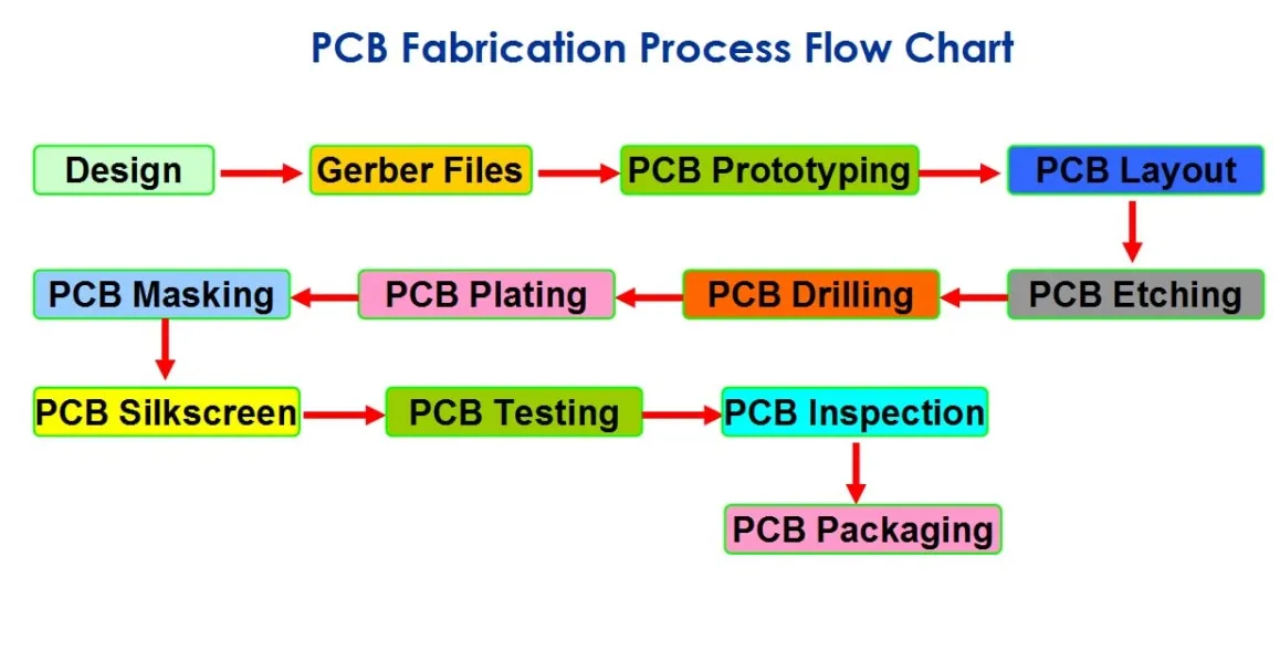
Phase 1: Schematic Capture and Review Checklist
Begin prototyping with a meticulous schematic review to establish a solid foundation. Verify all component symbols match datasheets, confirming pin numbers, polarities, and package types. Check netlist connectivity for opens, shorts, and unintended ties, using connectivity tools to simulate electrical paths. Ensure power and ground distribution includes sufficient decoupling capacitors near ICs to stabilize voltage rails.
Power budget analysis confirms supply currents do not exceed regulator ratings, accounting for worst-case scenarios. Reference designators must uniquely identify components for BOM integration. Simulate critical circuits for timing and voltage levels, flagging potential issues like excessive voltage drops. Document any assumptions, such as operating temperatures, for later validation.
This phase prevents propagation of errors into layout. Common oversights include mismatched footprints or omitted pull-up resistors. A complete schematic review checklist includes verifying ESD protection on interfaces and fuse placements for overcurrent scenarios.
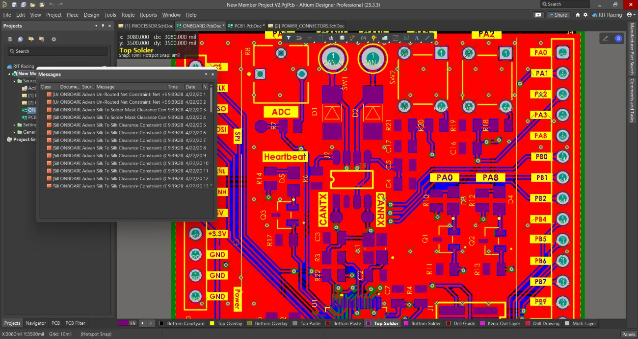
Phase 2: PCB Layout Verification Checklist
Transitioning to layout demands verification of placement and routing against schematic intent. Position components logically, grouping analog, digital, and power sections to minimize crosstalk. High-speed signals require controlled impedance routing with matched lengths for differential pairs. Verify trace widths meet current-carrying requirements, using calculators based on copper thickness and temperature rise.
Check clearances between traces, pads, and planes per voltage levels to prevent arcing. Vias must provide adequate annular rings, avoiding stubs that degrade signals. Ground planes should fill unused areas, with stitching vias for return paths. Review layer stackup for signal integrity, ensuring symmetric builds to control impedance.
Thermal hotspots from power devices need copper pours or vias for heat spreading. Component orientation facilitates assembly flow, aligning polarity marks consistently. Run design rule checks (DRC) for violations like minimum spacing. This PCB design checklist catches common PCB design mistakes such as acute angles creating acid traps during etching.
Phase 3: Design for Manufacturability (DFM) Checklist
A robust DFM checklist evaluates the design against fabrication and assembly capabilities before Gerber generation. Confirm minimum trace width and spacing suit the chosen process, typically starting at 4-5 mils for prototypes. Annular rings around vias and pads must exceed 3 mils to withstand drill breakout. Solder mask expansion prevents bridging, with openings aligned to pads.
Silkscreen legends avoid overlapping pads or traces, using fonts at least 6 mils tall for readability. Panelization rules include v-scoring or tab routing if multiples are ordered. Fiducials enable precise alignment for assembly. Board outline clearances from components prevent mechanical interference.
Drill sizes must be standard, with aspect ratios under 10:1 for reliability. Copper weight and finish selection, like HASL or ENIG, align with requirements. IPC-A-600 provides criteria for acceptability, guiding visual inspections. Addressing these in the PCB review process avoids PCB fabrication errors like slivers or mouse bites.
Phase 4: Gerber and Fabrication File Review
Generate Gerbers, drill files, and ODB++ with layer mapping verified against stackup. Use free viewers to inspect for missing layers or polarity errors. Bill of Materials (BOM) and pick-and-place files must match layout centroids accurately. Include fab notes specifying tolerances, such as bow and twist limits under 0.75%.
Perform a 3D render to check component heights against enclosure constraints. Cross-reference netlist post-export to confirm no changes. Submit test coupons for material characterization if high-reliability is needed. This step in the PCB design checklist ensures files communicate intent clearly.
During fabrication, incoming inspection verifies panel quantity, thickness, and markings. Post-etch checks per IPC-6012 confirm conductor widths and plating thickness. Electrical testing probes nets for continuity and isolation. Bare board visuals scan for voids, lifts, or warpage.
Common PCB Design Mistakes and Prevention Strategies
Among prevalent issues, poor component placement leads to signal integrity problems from excessive loop areas. Prevent by zoning sections and minimizing trace lengths. Inadequate power distribution causes voltage droops; counter with wide planes and bypass caps. Thermal mismanagement results in hotspots; incorporate simulations early.
Routing errors like non-orthogonal angles form acid traps, etching unevenly. Use 45-degree bends or curves instead. Ignoring via farm placement strains transitions; distribute evenly. Overcrowded layouts complicate rework; maintain 0.5 mm edge clearance.
Neglecting DFM yields fabrication errors such as insufficient annular rings causing drill breakout. Always run fab-specific DRCs. Weak solder joints from pad misalignment arise in assembly; verify footprints per IPC standards. A holistic PCB review process integrates these preventions.
Conclusion
Mastering error-free PCB prototyping hinges on a disciplined checklist from schematic to fabrication. Each phase builds reliability, averting common PCB design mistakes and PCB fabrication errors. Electrical engineers streamline workflows by embedding these verifications routinely. Adopting a DFM checklist enhances manufacturability, aligning prototypes with production realities. Prioritize reviews to minimize iterations and boost confidence in designs.
FAQs
Q1: What is a PCB design checklist and why use it in prototyping?
A1: A PCB design checklist systematically verifies schematic, layout, and DFM aspects to catch errors early. It prevents common PCB design mistakes like connectivity issues or clearance violations, saving time and costs. For electrical engineers, it ensures signal integrity and compliance, facilitating smooth transitions to fabrication. Regular use standardizes processes across teams.
Q2: What are the most frequent PCB fabrication errors and how to avoid them?
A2: Common PCB fabrication errors include insufficient annular rings, solder mask misalignment, and warpage from asymmetric stackups. A thorough DFM checklist addresses these by specifying tolerances and standard drill sizes. Pre-fab reviews confirm Gerber integrity, while standards like IPC-A-600 guide inspections. Incoming checks verify material specs.
Q3: How does a PCB review process integrate with the DFM checklist?
A3: The PCB review process incorporates DFM checklists to evaluate manufacturability post-layout. It flags issues like trace spacing or via placement against fab limits. Logical sequencing from schematic to files ensures holistic coverage. This prevents delays, aligning designs with process capabilities for prototypes.
Q4: What role do industry standards play in the PCB design checklist?
A4: Standards like IPC-6012 define performance specs for rigid boards, embedding criteria into checklists for conductor integrity and plating. They provide benchmarks for clearances and testing, reducing risks. Engineers reference them non-adjacently across phases for consistent quality.
References
IPC-6012F — Qualification and Performance Specification for Rigid Printed Boards. IPC, 2023
IPC-A-600M — Acceptability of Printed Boards. IPC, 2025
IPC-2221B — Generic Standard on Printed Board Design. IPC, 2012


