ALLPCB


Gaming PCs demand printed circuit boards that handle high-speed data transfer, substantial power delivery, and sustained thermal loads. These requirements drive the need for specialized pcb fabrication techniques for gaming pcs that deliver reliability and performance under demanding conditions. Engineers focus on multilayer constructions, precise material selection, and controlled processes to meet signal integrity and mechanical stability goals. High-performance systems often incorporate multiple layers to route complex interconnects while maintaining impedance control and minimizing crosstalk. Fabrication choices directly influence overall system stability during extended operation.
Why Multilayer PCB Fabrication Matters in Gaming Systems
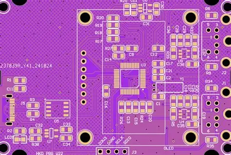
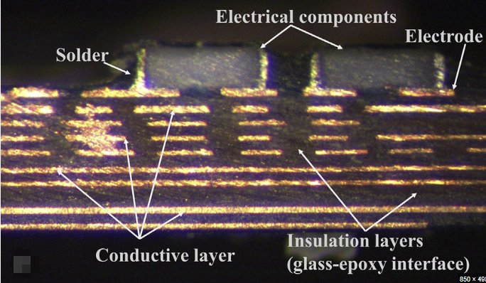
Multilayer pcb fabrication enables the dense routing required for modern graphics processing units, central processors, and high-speed memory interfaces. Gaming hardware typically operates at elevated clock frequencies where even minor deviations in trace geometry or dielectric properties can degrade signal quality. Fabricators build these boards by laminating multiple copper-clad cores with prepreg bonding sheets under controlled heat and pressure cycles. The resulting stackup supports power and ground planes that reduce noise and improve current-carrying capacity. Industry standards such as IPC-6012E guide qualification testing for these rigid multilayer constructions to verify electrical and mechanical performance.
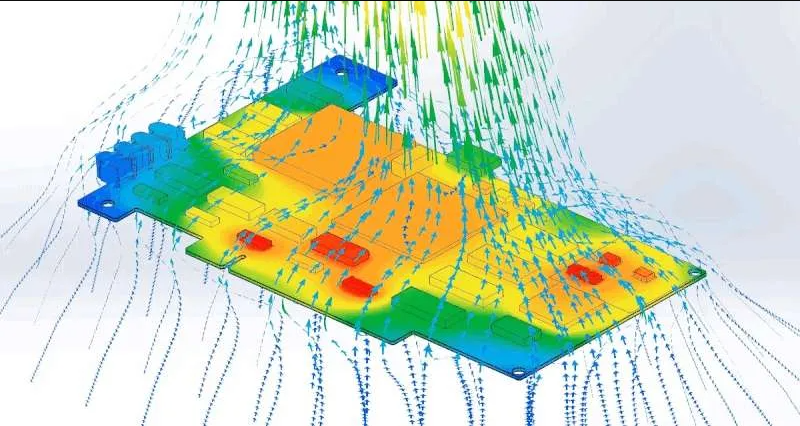
High layer counts also allow separation of analog, digital, and power domains, which helps maintain clean signal paths in mixed-signal gaming boards. Thermal management benefits from embedded copper planes that distribute heat away from critical components. Fabricators must balance layer count against overall board thickness to avoid excessive warpage during subsequent assembly steps.
High-Precision PCB Manufacturing Requirements
High-precision pcb manufacturing begins with accurate artwork generation and continues through imaging, etching, and plating operations. Gaming applications frequently require fine line widths and tight spacing to accommodate high pin-count devices and differential pairs. Photolithographic processes transfer circuit patterns onto copper surfaces with sub-micron registration accuracy. Subsequent etching removes unwanted copper while preserving the designed trace profiles. Controlled etch factors and undercut compensation ensure consistent impedance across critical nets.
Dimensional stability of the base materials becomes critical when boards undergo multiple thermal cycles. Fabricators select laminates with low coefficient of thermal expansion to minimize registration shifts between layers. Automated optical inspection verifies feature sizes and detects defects before proceeding to drilling and plating.
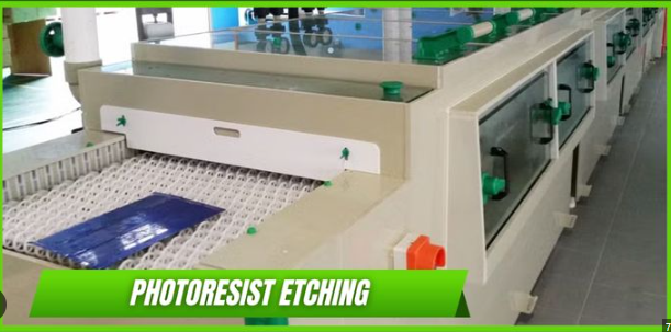
PCB Etching Process Details
The pcb etching process chemically removes copper from unwanted areas after the resist pattern has been developed. Alkaline or acidic etchants are applied in conveyorized systems that maintain consistent chemistry, temperature, and spray pressure. Undercut must be minimized to preserve trace width and edge definition, especially on fine features used in high-speed gaming circuits. Differential etching rates between copper and resist can affect final geometry, requiring process adjustments based on copper thickness and line density.
Post-etch cleaning removes residues that could interfere with subsequent plating or solder mask application. Etch compensation calculations performed during artwork preparation account for expected material removal to meet final dimensional tolerances. Consistent etch control supports the tight tolerances needed for controlled impedance traces in gaming motherboards and graphics cards.
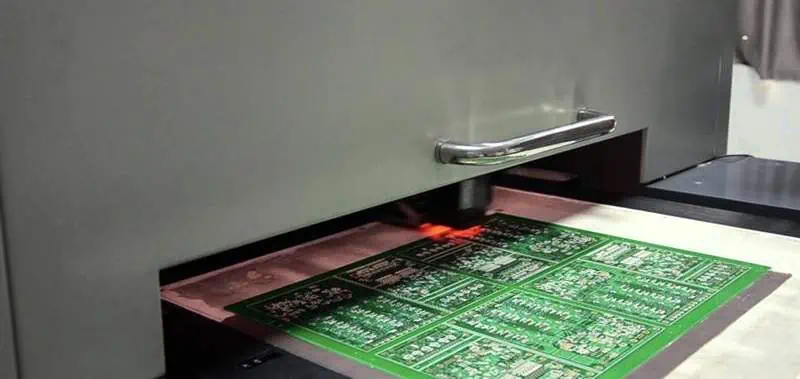
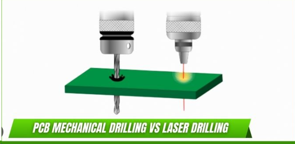
PCB Drilling Techniques for Complex Boards
Pcb drilling techniques create the vias and mounting holes essential for interlayer connections and component attachment. Mechanical drilling remains the primary method for through-holes, using carbide bits at controlled feed rates and spindle speeds to minimize smear and burring. For gaming boards with dense via fields, laser drilling produces microvias in blind or buried configurations that increase routing density without consuming surface real estate. Entry and exit materials protect the board surface and reduce exit burr formation during mechanical operations.
Hole wall quality directly affects plating adhesion and reliability under thermal stress. Deburring and desmear processes follow drilling to prepare surfaces for electroless copper deposition. Aspect ratio limits and minimum hole diameters are established according to board thickness and layer count to ensure complete plating coverage.
Quality Considerations and Best Practices
Quality control integrates throughout fabrication to verify compliance with performance specifications. Visual and automated inspection at multiple stages catches deviations before they propagate. Electrical testing confirms continuity and isolation across all nets. Thermal cycling and warpage measurements assess mechanical integrity after lamination and drilling. Adherence to IPC-A-600K provides acceptance criteria for surface and internal features that support long-term reliability in gaming environments.
Process controls on etch chemistry, drill parameters, and lamination cycles reduce variability. Material lot traceability and incoming inspection further support consistent output. These practices help ensure that fabricated boards meet the electrical, thermal, and mechanical demands of high-performance gaming hardware.
Conclusion
Effective pcb fabrication techniques for gaming pcs combine multilayer construction, precise etching, and controlled drilling to produce boards capable of supporting advanced processors and high-speed interfaces. Attention to material properties, process parameters, and inspection protocols delivers the reliability required for sustained operation. Engineers who understand these fabrication fundamentals can better specify requirements that align with system performance targets.
FAQs
Q1: What distinguishes multilayer pcb fabrication for gaming applications from standard boards?
A1: Multilayer pcb fabrication for gaming pcs incorporates additional signal, power, and ground layers to support high-speed routing and thermal management. These constructions require precise lamination cycles and impedance control not always needed in lower-performance products. The added complexity demands tighter process controls to maintain registration and electrical performance.
Q2: How does the pcb etching process affect high-speed signal integrity in gaming hardware?
A2: The pcb etching process determines final trace geometry and edge definition, both of which influence impedance and crosstalk in high-frequency circuits. Consistent etch control preserves designed line widths and minimizes undercut that could alter electrical characteristics. Gaming systems benefit from etch processes tuned for fine features and uniform results across the panel.
Q3: Why are specialized pcb drilling techniques important for multilayer gaming boards?
A3: Specialized pcb drilling techniques create reliable interlayer connections while accommodating dense via patterns required by complex gaming designs. Mechanical and laser methods each address different via types, and proper parameter selection prevents defects that could compromise electrical or mechanical integrity. Controlled drilling supports the high layer counts typical in performance-oriented motherboards and add-in cards.
Q4: What role does high-precision pcb manufacturing play in thermal performance of gaming systems?
A4: High-precision pcb manufacturing ensures accurate placement of copper planes and thermal vias that aid heat spreading in gaming hardware. Consistent layer registration and feature definition allow designers to implement effective thermal management strategies without unexpected impedance or mechanical issues. Precise fabrication supports the power delivery and cooling requirements of high-wattage components.
References
IPC-6012E — Qualification and Performance Specification for Rigid Printed Boards. IPC, 2017
IPC-A-600K — Acceptability of Printed Boards. IPC, 2020
JEDEC J-STD-020E — Moisture/Reflow Sensitivity Classification. JEDEC, 2014