 ALLPCB


Cost vs. Performance: Finding the Right Solder Mask Thickness for Your Budget
In PCB manufacturing, engineers and procurement teams frequently evaluate solder mask thickness as a key variable that influences both overall project costs and long-term board reliability. Thicker solder mask layers require additional material and processing steps, which directly raise manufacturing cost, while thinner layers help control PCB budget but may limit environmental protection and electrical performance. The decision often centers on solder mask thickness cost trade-offs that affect everything from initial fabrication expenses to field durability. For electric engineers working on designs that range from consumer electronics to industrial controls, understanding these relationships supports informed choices that align with specific application demands and available resources. Proper selection contributes to PCB cost optimization without compromising essential functionality.
What Is Solder Mask Thickness and Why It Matters
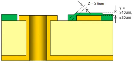
Solder mask thickness refers to the cured coating applied over copper traces and substrate to provide insulation and protection during assembly and operation. Typical values fall within ranges established by industry guidelines, where the layer must cover conductors adequately while allowing for component placement and soldering processes. This dimension matters because it affects dielectric spacing, moisture resistance, and mechanical stability of the finished board. In budget-conscious projects, variations in thickness influence solder mask material cost and overall manufacturing cost, prompting teams to assess requirements early in the design phase. Electric engineers consider these factors when prioritizing PCB budget allocation across multiple board revisions or production volumes.
Technical Principles of Solder Mask Thickness
The thickness of the solder mask layer determines its ability to act as a dielectric barrier between conductors and external elements. A greater thickness generally increases insulation resistance and reduces the risk of electrical shorts under humid or contaminated conditions. However, excessive thickness can alter high-frequency signal behavior by changing effective dielectric constants and trace impedance in controlled-impedance designs. Application methods such as screen printing or spray coating influence achievable uniformity, with thicker deposits sometimes leading to uneven surfaces that affect subsequent assembly steps. Standards from IPC provide guidance on minimum coverage and performance expectations for rigid boards, helping engineers quantify acceptable limits without over-specifying material usage.
Mechanical considerations also come into play, as thicker masks can contribute to board warpage during thermal cycling due to differences in coefficient of thermal expansion between the mask and substrate. This effect becomes more pronounced in larger panels or boards with asymmetric copper distribution. Conversely, thinner masks reduce material volume and associated stresses but offer less margin against abrasion or chemical exposure during manufacturing and use. Electric engineers evaluate these interactions through simulation and prototype testing to predict impacts on both electrical performance and long-term reliability.
Practical Approaches to Balancing Cost and Performance
Engineers begin by defining the operating environment and electrical requirements for each design. Boards intended for harsh conditions may justify increased thickness to enhance protection, whereas high-volume consumer products often favor thinner layers to minimize solder mask material cost and support PCB cost optimization. Collaboration between design and manufacturing teams helps identify the minimum thickness that satisfies performance criteria while controlling manufacturing cost. Documentation of these decisions supports consistent results across production runs and facilitates future revisions when budgets or specifications change.
Testing protocols verify that chosen thicknesses meet insulation and coverage needs without introducing assembly issues. Electric engineers review supplier capabilities for coating uniformity and curing consistency, as these factors directly affect yield and rework rates. In many cases, standard thicknesses align with common IPC acceptance criteria, allowing teams to avoid custom processes that inflate expenses. Adjustments during the quoting stage can reveal opportunities to reduce PCB budget by relaxing non-critical thickness tolerances where electrical margins permit.
Best Practices for Budget-Conscious Selection
Start with application-specific requirements rather than defaulting to maximum thickness. Review trace spacing, voltage levels, and expected environmental exposure to establish a baseline. Then compare the incremental cost of additional mask material against projected improvements in reliability or reduced failure rates. Electric engineers often document these analyses to justify decisions to procurement and management stakeholders focused on overall project economics.
Consider panel-level processing efficiencies, as thicker masks may require slower application speeds or additional passes that extend cycle time. Where fine-pitch components are present, thinner masks can improve solder paste release and reduce bridging risks during reflow. Regular review of process capability data helps maintain consistency while identifying opportunities for further PCB cost optimization without sacrificing quality.
Conclusion
Selecting solder mask thickness requires careful evaluation of performance needs against direct impacts on manufacturing cost and solder mask material cost. Electric engineers who integrate these considerations early in the design cycle achieve better PCB budget control while meeting reliability targets. Consistent application of industry guidelines supports repeatable outcomes across different production scenarios. Ultimately, the right choice reflects a balanced assessment of electrical, mechanical, and economic factors specific to each project.
FAQs
Q1: How does solder mask thickness affect PCB manufacturing cost?
A1: Solder mask thickness influences manufacturing cost through material volume and processing time. Thicker layers require more coating material and potentially additional application or curing steps, raising expenses. Electric engineers review these variables during quoting to align thickness with project budget constraints while maintaining necessary protection levels.
Q2: What role does solder mask thickness play in PCB cost optimization?
A2: Solder mask thickness contributes to PCB cost optimization by allowing designers to specify only the coverage needed for the application. Reducing unnecessary thickness lowers material usage and can improve yield in high-volume runs. Teams balance this against performance requirements to achieve overall budget targets without compromising board functionality.
Q3: Can solder mask material cost be reduced without affecting performance?
A3: Solder mask material cost can often be managed by selecting the minimum thickness that satisfies electrical insulation and environmental protection needs. Electric engineers consult process data and acceptance criteria to confirm that thinner options remain viable. This approach supports budget goals while preserving essential board characteristics.
Q4: How do industry standards guide solder mask thickness decisions?
A4: Industry standards outline minimum coverage and performance expectations that help define appropriate thickness ranges. Electric engineers reference these guidelines to ensure designs meet qualification requirements without over-specifying material. Such references promote consistency and support informed cost-performance trade-offs across different board types.
References
IPC-6012E — Qualification and Performance Specification for Rigid Printed Boards. IPC, 2017
IPC-A-600K — Acceptability of Printed Boards. IPC, 2020
IPC-SM-840E — Qualification and Performance Specification of Permanent Solder Mask and Flexible Cover Materials. IPC, 2010


