 ALLPCB


Introduction
High-density interconnect (HDI) assembly enables compact electronics with superior signal integrity and component density, making it essential for modern devices like smartphones and medical equipment. However, the complexity of HDI processes often drives up costs, challenging engineers to balance high performance with budget constraints. HDI assembly cost optimization becomes critical when projects demand reliability without excessive spending. Engineers must navigate trade-offs in design, materials, and manufacturing to achieve efficient outcomes. This article explores practical strategies for cost-effective HDI assembly, drawing on industry-proven approaches tailored for electrical engineers.
Understanding HDI Assembly and Its Cost Drivers
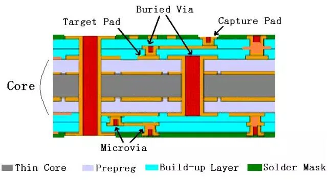
HDI assembly involves soldering fine-pitch components onto boards featuring microvias, blind vias, and buried vias, which allow for denser routing compared to standard multilayer boards. These features support higher I/O counts and reduced signal path lengths, improving electrical performance in high-speed applications. Costs arise primarily from advanced fabrication steps like laser drilling, sequential lamination, and precise plating, which require specialized equipment and skilled labor. Material selection HDI cost plays a significant role, as premium dielectrics and copper foils add to expenses. Without careful planning, yields drop due to defects like via misalignment or warpage, further inflating overall project budgets. Electrical engineers must identify these drivers early to implement targeted optimizations.
Key Factors Influencing HDI Assembly Costs
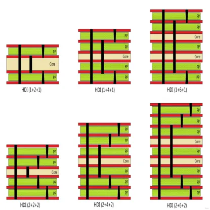
Layer Count and Stackup Optimization
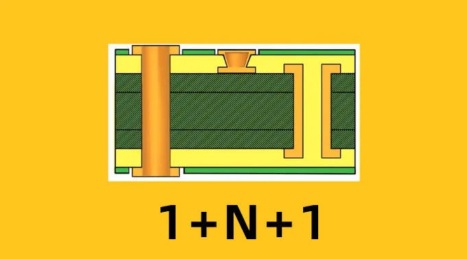
Layer count directly impacts HDI assembly costs, as each additional layer increases material usage, lamination cycles, and registration challenges. Reducing layers through efficient routing preserves functionality while cutting expenses on core materials and buildup processes. Stackup design influences thermal management and signal integrity, where unbalanced configurations lead to higher defect rates during assembly. Engineers can minimize layers by grouping signals logically and leveraging microvias for interlayer connections. HDI design for cost starts here, prioritizing minimal buildup classes like 1+n+1 over complex stacked structures. Proper stackup planning aligns with IPC-2226 guidelines for reliable, economical layouts.
Material Selection for Cost Control
Material selection HDI cost hinges on choosing dielectrics with adequate glass transition temperature (Tg) and low coefficient of thermal expansion (CTE) without over-specifying for the application. Standard FR-4 cores suffice for many designs, avoiding pricier high-Tg or low-loss variants unless high-speed signals demand them. Thinner cores reduce material volume and improve via aspect ratios, easing plating processes. Copper foil weight also matters; lighter foils lower costs but require verification for current-carrying capacity. Engineers troubleshoot material-related issues by matching CTE between layers to prevent delamination during reflow. This approach ensures performance without unnecessary premiums.
Via Structures and Process Complexity
Via types dominate HDI manufacturing costs, with stacked and staggered microvias adding steps like multiple laser drills and fills. Preferring staggered vias over stacked reduces buildup iterations, simplifying sequential lamination and boosting throughput. Mechanical drilling for larger vias cuts laser usage, a major expense driver. Aspect ratios must stay below recommended limits to avoid plating voids, which cause assembly failures. HDI manufacturing efficiency improves by standardizing via sizes and minimizing unique layer pairs. Troubleshooting via reliability involves inspecting fill quality to avoid cracks under thermal cycling.
Strategies for HDI Assembly Cost Optimization
HDI Design for Cost: Layout Best Practices
Start HDI design for cost by optimizing component placement to shorten traces and reduce vias. Place high-density ICs centrally, routing signals in fewer layers with fine-line rules. Use via-in-pad judiciously for BGA escapes, ensuring dog-bone shapes prevent solder wicking. Simulate signal integrity early to validate reductions in layer count. Panel utilization matters; design for standard panel sizes to minimize scrap. These practices yield higher assembly success rates and lower per-unit costs.
Layer Count Reduction Techniques
Layer count reduction transforms costly HDI boards into budget-friendly alternatives without sacrificing density. Consolidate power and ground planes, using embedded passives where feasible to free routing space. Microvias enable every-layer connections, often halving traditional layer needs. Review netlists for redundant routing, merging where impedance allows. Electrical engineers troubleshoot by iterating stackups in design tools, targeting buildups like 4-6-4. This strategy enhances overall HDI manufacturing efficiency.
Material Selection HDI Cost Strategies
Target material selection HDI cost by selecting resins with balanced Dk/Df for the frequency range, avoiding ultra-low loss unless critical. Low-cost prepregs with controlled flow prevent resin squeeze-out during lamination. Verify supplier data for via laser ablation rates to ensure clean drilling. Hybrid stackups mix standard and advanced materials strategically. Cost audits reveal savings from bulk ordering common thicknesses. Practical testing confirms assembly compatibility under reflow profiles.
Enhancing HDI Manufacturing Efficiency
Streamline HDI manufacturing efficiency through process standardization, such as fixed sequential lamination cycles tailored to buildup class. Automate inspections post-lamination to catch registration errors early, preserving yield. Optimize plating baths for uniform copper deposition in microvias, reducing rework. IPC-6016 qualification specs guide acceptance criteria, ensuring consistent quality. Collaborate with fabricators on design rules to align capabilities. Troubleshooting efficiency bottlenecks involves yield data analysis per process step.
Best Practices for Assembly Process Control
Assembly demands precision for fine-pitch BGAs and LGAs on HDI boards. Follow J-STD-001 requirements for soldering profiles to prevent microvia damage from overheating. Solder paste selection affects stencil release, critical for 0.3mm pitches. Reflow optimization minimizes warpage, using fixtures for flatness. Post-assembly X-ray verifies joint integrity without invasive tests. These practices support HDI assembly cost optimization by reducing escapes.
Troubleshooting Common Cost Overruns in HDI Assembly
Overruns often stem from via fill failures, leading to open circuits post-assembly. Inspect laser drills for taper and cleanliness to avoid plating defects. Warpage from asymmetric stackups causes stencil misalignment; balance copper distribution. Excessive stacked vias inflate lamination costs; convert to staggered where possible. Yield drops from poor material adhesion signal CTE mismatch. Systematic DFM reviews catch these early, restoring budget control.
Conclusion
Cost-effective HDI assembly requires integrated efforts in design, materials, and processes to balance performance and budget. Key wins come from layer count reduction, strategic material selection HDI cost, and HDI manufacturing efficiency gains. Adhering to standards like IPC-2226 ensures reliability. Electrical engineers achieve optimal results by troubleshooting proactively and iterating designs. Implementing these strategies delivers high-density boards that meet specs economically.
FAQs
Q1: How does layer count reduction impact HDI assembly cost optimization?
A1: Layer count reduction lowers material and lamination expenses while simplifying assembly handling. By optimizing routing with microvias, engineers cut buildups from 12+ to 8 layers, boosting yield and throughput. This maintains signal integrity for high-speed apps. Practical designs group signals efficiently, aligning with IPC guidelines for cost savings without performance loss.
Q2: What role does material selection play in HDI cost?
A2: Material selection HDI cost focuses on standard dielectrics with sufficient Tg/CTE for reliability. Avoid over-specifying low-Dk materials unless needed, opting for cost-effective cores. Thinner prepregs reduce volume and improve via ratios. Test compatibility to prevent delamination during assembly. Balanced choices yield 10-20% savings in prototypes.
Q3: How to improve HDI manufacturing efficiency?
A3: HDI manufacturing efficiency rises through standardized sequential lamination and via optimization. Prefer staggered microvias to minimize cycles, enhancing yield. Automate inspections and align designs with fab capabilities. J-STD-001 compliance ensures assembly smoothness. Data-driven process tweaks address bottlenecks effectively.
Q4: What are essential HDI design for cost tips?
A4: HDI design for cost emphasizes minimal layer pairs, efficient placement, and standard via sizes. Use via-in-pad sparingly with proper escapes. Simulate stackups for balance. Panelize for utilization. These reduce fabrication steps and assembly risks, delivering budget-friendly high-performance boards.


