ALLPCB


Introduction
Crystal oscillators serve as the heartbeat of wireless communication systems, delivering precise frequency references that underpin everything from data transmission to synchronization. In modern wireless devices, such as routers, base stations, and IoT modules, these components ensure that signals remain accurate amid environmental challenges like temperature fluctuations and electromagnetic interference. Engineers designing crystal oscillator wireless integrations prioritize stability to maintain reliable performance across RF bands. Poor frequency control can lead to degraded signal quality, increased bit error rates, and compliance failures in spectrum usage. This article explores the role of crystal oscillators in RF applications, focusing on signal integrity, phase noise, and jitter management. By understanding these elements, electric engineers can optimize PCB layouts for superior wireless functionality.
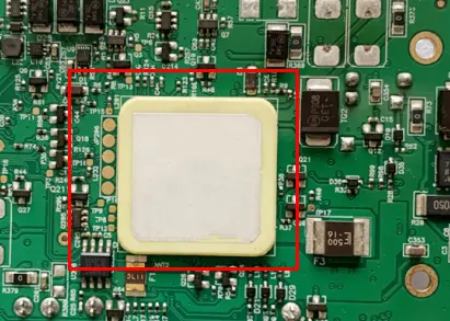
Wireless systems demand clock sources with exceptional purity because even minor instabilities amplify in up-conversion chains. Crystal oscillators excel here due to their high quality factor, which minimizes energy loss and sustains oscillation. As bandwidths expand in 5G and beyond, the need for low crystal oscillator phase noise becomes critical to avoid spectral regrowth. This guide draws on engineering principles to provide practical insights for implementation.
What Is a Crystal Oscillator and Why It Matters in Wireless Communication
A crystal oscillator generates a stable electrical signal using the piezoelectric properties of quartz crystals, vibrating at a precise resonant frequency when voltage is applied. This mechanical resonance converts to an electrical output, offering far superior stability compared to RC or LC oscillators. In wireless communication, crystal oscillators provide the reference clock for phase-locked loops (PLLs), mixers, and modulators, ensuring carrier frequencies align accurately. Without this precision, transceivers cannot lock onto channels or demodulate signals effectively, leading to dropped connections and reduced throughput.
The importance of crystal oscillator wireless setups lies in their ability to support high-data-rate protocols like Wi-Fi, Bluetooth, and cellular standards. These systems operate in crowded spectrum environments where frequency accuracy prevents interference and enables efficient power use. Engineers select crystals based on fundamental mode operation to achieve low spurious responses, vital for clean RF output. Moreover, in battery-powered devices, their low power draw while maintaining stability makes them indispensable.
Crystal oscillators also enable time-division duplexing and frequency hopping, where timing precision dictates performance. Instabilities manifest as phase errors, degrading eye diagrams and increasing error vector magnitude. By anchoring the local oscillator chain, they ensure signal accuracy across varying conditions, making them a cornerstone of reliable wireless links.
Principles of Crystal Oscillator Operation in RF Applications
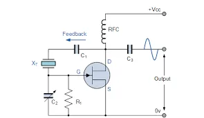
Crystal oscillators in RF circuits typically employ configurations like the Pierce or Colpitts topology, where the quartz crystal acts as the frequency-determining element in a feedback loop. The crystal's high Q-factor, often exceeding thousands, results in sharp resonance peaks that reject nearby frequencies, ideal for crystal oscillator RF purity. Amplifiers sustain oscillation by compensating for losses, while capacitors tune the load to match the crystal's specifications. This setup produces a sinusoidal output suitable for driving digital dividers or analog multipliers in wireless transceivers.
Environmental factors influence operation, as mechanical stress or thermal expansion alters the crystal's cut angle and resonance. Oven-controlled variants stabilize temperature for demanding base stations, but standard AT-cut crystals suffice for most mobile applications. In PCB contexts, proper drive level prevents overdriving, which shifts frequency and introduces harmonics. Adhering to design guidelines from IPC-2221 helps mitigate these effects through controlled trace routing and component spacing.
The inverse piezoelectric effect closes the loop, converting electrical energy back to mechanical vibrations for self-sustaining operation. Load capacitance mismatches cause pulling, where frequency deviates from nominal, impacting PLL lock times. Engineers calculate equivalent series resistance to ensure startup reliability under capacitive loads.
Key Performance Metrics: Phase Noise, Jitter, and Signal Integrity
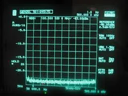
Phase noise represents random fluctuations in the oscillator's phase, appearing as sidebands in the frequency domain that mask weak signals in wireless receivers. Close-in phase noise affects carrier recovery, while floor noise limits sensitivity in narrowband systems. Crystal oscillator phase noise performance stems from the quartz's mechanical isolation from electronic noise, outperforming synthesized sources. Low phase noise preserves modulation accuracy, reducing adjacent channel interference in dense deployments.
Jitter quantifies timing variations in the time domain, correlating directly with phase noise via Fourier transforms. Cycle-to-cycle jitter dominates in bursty wireless protocols, while accumulated jitter impacts long-term synchronization. Crystal oscillator jitter minimization requires clean power supplies and short traces to avoid coupling from digital switching. High jitter elevates bit error rates by smearing clock edges, compromising data recovery.
Signal integrity ties these metrics together, as PCB parasitics couple noise into the oscillator loop. Crystal oscillator signal integrity suffers from ground bounce or supply ripple, manifesting as spurs. Shielding and filtering preserve waveform fidelity, ensuring downstream RF chains perform as specified. Metrics like Allan variance further characterize long-term stability for GPS receivers.
PCB Design Best Practices for Crystal Oscillators in Wireless Modules
Optimal PCB layout positions the crystal oscillator close to the host IC to minimize trace inductance, which can detune the circuit. Dedicated ground vias under the crystal form a solid plane, shunting noise to return paths per IPC-2221 guidelines. Decoupling capacitors, placed within millimeters of power pins, filter high-frequency ripple, stabilizing the loop. Guard traces or moats isolate the oscillator from aggressive digital signals, preserving crystal oscillator RF integrity.
Component selection involves matching load capacitance precisely to avoid frequency pulling, verified through simulation. Vias and stitching enhance return currents, reducing loop area for EMI susceptibility. In multilayer boards, dedicate inner layers for ground shielding the oscillator section. Ferrite beads on supplies attenuate conducted noise without degrading transient response.
Thermal management prevents convection-induced drifts; vias to heat sinks or copper pours dissipate heat evenly. Compliance with J-STD-001 during assembly ensures solder joints withstand vibration, common in wireless handsets. Testing involves spectrum analysis for phase noise and time-interval error for jitter, confirming design margins.
Multiband wireless demands multiple oscillators; careful zoning prevents crosstalk. Symmetrical routing balances differential outputs if applicable.
Common Challenges and Troubleshooting in Crystal Oscillator Wireless Integration
Startup failures often trace to insufficient drive or capacitive mismatch; measure ESR to diagnose. Excessive phase noise indicates power supply coupling, remedied by improved PDN design. Jitter spikes correlate with PCB flexure, addressed via mounting pads per assembly standards. Environmental testing reveals acceleration sensitivity, mitigated by soft damping materials.
Intermittent lock loss in PLLs stems from crystal oscillator signal integrity degradation over temperature. Oscilloscope captures reveal waveform distortion from poor grounding. Firmware adjustments for pull range help, but hardware fixes yield permanence. Vibration profiles simulate field use, ensuring reliability.
Troubleshooting flowcharts start with visual inspection, progressing to parametric sweeps. Documentation of parasitics aids iterations.
Conclusion
Crystal oscillators remain vital for wireless communication, delivering the accuracy needed for phase noise, jitter control, and signal integrity. PCB engineers achieve reliability through principled layout, standards adherence, and rigorous verification. As wireless evolves, these components will anchor next-generation systems. Prioritizing crystal oscillator wireless best practices ensures robust performance.
FAQs
Q1: What role does a crystal oscillator play in maintaining RF signal integrity?
A1: Crystal oscillators provide a stable frequency reference that minimizes phase perturbations in RF chains. Low crystal oscillator signal integrity issues like spurs or distortion arise from layout errors, resolved by solid grounding and decoupling. This preserves modulation quality in wireless transceivers, reducing error rates.
Q2: How does crystal oscillator phase noise impact wireless performance?
A2: Phase noise introduces spectral sidebands that degrade receiver sensitivity and increase interference. In crystal oscillator RF applications, superior quartz stability keeps noise low, supporting high-order modulation. Engineers specify based on link budget to meet system requirements.
Q3: Why is jitter a critical concern for crystal oscillator wireless systems?
A3: Jitter causes timing uncertainty, affecting clock recovery and synchronization in packet-based networks. Crystal oscillator jitter from supply noise or mechanical shock worsens bit errors. Mitigation via clean PCB design ensures reliable data throughput.
Q4: What PCB practices improve crystal oscillator reliability?
A4: Place crystals near ICs with ground planes and decoupling per IPC standards. This cuts parasitics, enhancing crystal oscillator phase noise and jitter. Assembly per J-STD-001 prevents joint failures under stress.
References
IPC-2221 — Generic Standard on Printed Board Design. IPC, 2003
J-STD-001 — Requirements for Soldered Electrical and Electronic Assemblies. IPC/JEDEC, 2020
IEC 60679-1 — Quartz crystal controlled oscillators of assessed quality. IEC, 2007