 ALLPCB


Introduction
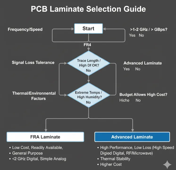
Standard FR-4 laminates have served the PCB industry reliably for decades in low to moderate frequency applications. However, as designs push into high-frequency realms such as 5G, radar systems, and satellite communications, FR-4's limitations become evident. Signal integrity degrades due to higher dielectric losses and inconsistent electrical properties at frequencies above 1 GHz. Electrical engineers must select specialized high frequency PCB materials to maintain performance. This RF laminate selection guide explores alternatives, key properties, and practical considerations for optimal choices. Understanding these factors ensures reliable operation in demanding RF environments.
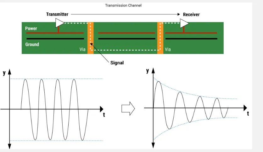
Limitations of FR-4 in High-Frequency Applications
FR-4, a fiberglass-reinforced epoxy, exhibits a dielectric constant (Dk) around 4.4 and dissipation factor (Df) of about 0.02 at microwave frequencies. These values lead to significant signal attenuation and phase shifts as frequency increases beyond 1 GHz. The material's Dk varies with frequency and temperature, causing impedance mismatches in transmission lines. Moisture absorption further exacerbates losses, altering electrical characteristics during operation. For applications exceeding 7 GHz, FR-4 becomes unsuitable, prompting the shift to advanced RF laminates. Engineers observe these issues in simulations and prototypes, necessitating material upgrades for phase-stable performance.
High-frequency signals demand materials with minimal variation in propagation velocity. FR-4's higher Df converts more energy to heat, reducing efficiency in power-sensitive designs. Thermal expansion mismatches with copper also risk reliability in multilayer stacks. Industry standards like IPC-2221 emphasize material selection for controlled impedance and low loss. Transitioning beyond FR-4 preserves signal integrity across the board. This step is critical for modern RF systems where every dB of insertion loss matters.
Related Reading: Beyond FR-4: Choosing the Right PCB Laminate to Combat Delamination in Extreme Environments
Essential Properties of High-Frequency PCB Materials
Dielectric constant (Dk) measures a material's ability to store electrical energy, directly affecting signal speed and impedance. Ideal RF laminates target Dk values between 2.2 and 3.5 for controlled propagation in microstrip and stripline structures. Low Dk uniformity across the plane prevents skew in differential pairs. Engineers prioritize this for matching characteristic impedance over wide bandwidths. Dissipation factor (Df) quantifies energy loss, with premium materials achieving below 0.005, often under 0.002 at 10 GHz. These properties minimize insertion loss in antennas and filters.
Thermal stability ranks next, including coefficient of thermal expansion (CTE) matching copper's 17 ppm/°C in the Z-axis. Glass transition temperature (Tg) above 170°C supports lead-free soldering without degradation. Low moisture absorption, under 0.1%, maintains stable Dk during environmental exposure. Mechanical strength ensures drillability and plating adhesion in fabrication. IPC-6018D specifies qualification tests for these traits in high-frequency boards. Balancing these yields robust designs resilient to thermal cycling.
Frequency-dependent behavior requires Dk and Df stability from DC to millimeter waves. Temperature coefficients of Dk below 50 ppm/°C prevent detuning in phased arrays. Copper surface roughness impacts skin effect losses, favoring low-profile foils like reverse-treated or RTF. Electrical engineers evaluate datasheets for these metrics during selection. Comprehensive testing verifies real-world performance.
Types of RF Laminates and Material Examples
PTFE-based laminates form the backbone of ultra-high-frequency applications due to inherent low loss. Pure PTFE offers Dk around 2.1 and Df as low as 0.0003, but requires fillers for rigidity. Ceramic-filled PTFE composites, such as those in Rogers PCB material series like RO3003 or RO4350B, achieve Dk 3.0-3.5 with Df 0.001-0.004. These suit hybrid multilayers with FR-4 cores. Taconic PCB material options like TLX or RF-35 provide similar profiles, emphasizing low CTE for aerospace. Isola PCB material, including Astra or I-Tera series, bridges epoxy-like processability with RF performance.
Hydrocarbon or PPE-based laminates offer cost-effective alternatives for frequencies up to 20 GHz. These exhibit low Df around 0.003 and better mechanical stability than pure PTFE. LCP films excel in millimeter-wave with ultra-low Df but demand specialized handling. Each type trades process ease for electrical excellence. Rogers PCB material dominates in volume production for its consistency. Taconic and Isola variants cater to custom needs with tailored fillers.
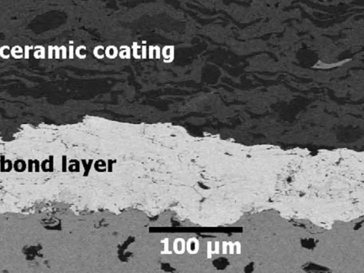
Hybrid constructions combine RF top layers with FR-4 interiors to optimize cost and performance. Selection hinges on application bandwidth and power handling.
RF Laminate Selection Guide: Key Factors
Frequency range dictates primary choice; below 10 GHz, ceramic-PTFE suffices, while mmWave favors pure PTFE or LCP. Power applications prioritize thermal conductivity above 0.5 W/mK and high breakdown voltage. Environmental factors like operating temperature from -55°C to 125°C demand low Z-CTE variation. Fabrication compatibility influences decisions, as PTFE requires special drilling and lamination. IPC-6012E outlines performance specs for rigid boards incorporating these materials. Engineers simulate stackups to validate choices early.
Cost of RF PCB escalates with material price, often 5-10 times FR-4 due to raw material and processing. Raw laminate costs range higher for low-Df variants, compounded by yield sensitivities. Volume production mitigates this through hybrids. Taconic PCB material may offer 10-20% savings over premium Rogers options in prototypes. Total board cost includes via reliability and test fixtures. Balancing performance against budget requires trade-off analysis.
- Factor: Dk Target — Low-Frequency RF (<10 GHz): 3.0-3.5; High-Frequency RF (>20 GHz): 2.2-2.6
- Factor: Df Max — Low-Frequency RF (<10 GHz): 0.004; High-Frequency RF (>20 GHz): 0.002
- Factor: Cost Relative to FR-4 — Low-Frequency RF (<10 GHz): 3-5x; High-Frequency RF (>20 GHz): 8-15x
- Factor: Example Materials — Low-Frequency RF (<10 GHz): Rogers RO4000, Isola Astra; High-Frequency RF (>20 GHz): Taconic TLX, Pure PTFE
Impedance control tolerances tighten to ±5% for RF traces. Signal integrity tools predict losses pre-layout.
Related Reading: The Ultimate Guide to RF Laminate PCB Stack Up Design for Signal Integrity
Best Practices for Implementation
Qualify laminates per IPC-6018D through thermal shock, S-parameter testing, and TCT. Hybrid stackups layer RF materials strategically, bonding with compatible prepregs. Control copper roughness below 1.5 μm RMS for skin effect mitigation. Design ground planes with via stitching to suppress modes. Moisture preconditioning follows JEDEC J-STD-020E before assembly. These steps align with standards for repeatability.
Fabrication partners must handle low-loss materials to avoid drill wander or smear. Simulate phase stability across temperature sweeps. Field-replaceable units benefit from modular RF sections. Documentation includes material datasheets and stackup drawings. Post-production validation confirms low VSWR.
Conclusion
Selecting the right RF laminate transcends FR-4's capabilities for high-frequency success. Prioritize low, stable Dk/Df, thermal matching, and fab compatibility in your RF laminate selection guide. Examples like Rogers PCB material, Taconic PCB material, and Isola PCB material illustrate diverse options balancing performance and practicality. Cost of RF PCB demands strategic hybrids and volume planning. Adhering to IPC standards ensures qualified designs. Electrical engineers achieve superior signal integrity through informed choices.
FAQs
Q1: What are the primary differences between FR-4 and high frequency PCB materials?
A1: High frequency PCB materials feature lower Dk (2.2-3.5 vs 4.4) and Df (<0.005 vs 0.02), ensuring minimal signal loss above 1 GHz. They offer better thermal and moisture stability for consistent performance. FR-4 suits general use, while RF laminates target microwave applications per IPC-6018D guidelines. Selection depends on bandwidth needs.
Q2: How does cost of RF PCB compare to standard boards?
A2: RF PCB costs rise 5-15 times due to premium laminates and processing. Hybrids reduce expenses by limiting RF layers. Factors include volume, thickness, and copper type. Engineers optimize via stackup design for budget constraints without sacrificing integrity.
Q3: Which Rogers PCB material is best for 5G applications?
A3: Rogers series like RO4350B provide Dk 3.48 and low Df for sub-6 GHz 5G. They process like FR-4 with superior loss characteristics. Verify via simulations for your impedance. Hybrid use lowers overall cost of RF PCB.
Q4: What role does IPC-6018D play in RF laminate selection?
A4: IPC-6018D defines qualification for high-frequency boards, covering electrical, mechanical, and environmental tests. It guides acceptance criteria for low-loss laminates. Compliance ensures reliability in RF designs.
References
IPC-6018D — Qualification and Performance Specification for High-Frequency and Microwave Printed Boards. IPC.
IPC-2221G — Generic Standard on Printed Board Design. IPC.
IPC-6012E — Qualification and Performance Specification for Rigid Printed Boards. IPC, 2017.
JEDEC J-STD-020E — Moisture/Reflow Sensitivity Classification. JEDEC, 2014.





