 ALLPCB


Introduction
Electric vehicle adoption continues to accelerate, which increases demand for reliable onboard and offboard charging systems. Battery charger printed circuit boards form the core of these systems and must handle elevated voltages and currents while maintaining safety and long term performance. Engineers face distinct requirements when designing automotive PCBs for chargers compared with standard consumer electronics. High voltage PCB layouts require careful attention to insulation distances and material properties to prevent arcing or breakdown. High current PCB traces must carry substantial amperage without excessive heating or voltage drop. These factors make EV charger PCB design a specialized discipline within automotive electronics.
Why EV Charger PCB Design Matters
Effective EV charger PCB design directly influences charging speed, system efficiency, and overall vehicle safety. Automotive PCB assemblies operate in environments that include vibration, temperature cycling, and exposure to moisture or contaminants. Failures in charger electronics can lead to downtime, reduced battery life, or safety incidents. Compliance with recognized industry standards helps ensure consistent quality and performance across production batches. Manufacturers therefore prioritize designs that balance electrical performance with mechanical robustness and thermal stability. This focus supports the broader goals of reliable fast charging infrastructure and extended vehicle service life.
Key Challenges in High Voltage and High Current PCB Design
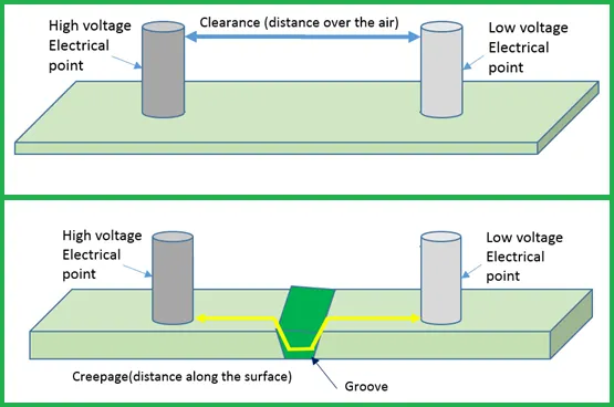
High voltage operation introduces risks of dielectric breakdown and surface tracking that demand increased creepage and clearance distances. High current paths generate significant heat, which can cause trace delamination or component failure if not managed through adequate copper thickness and thermal relief. Electromagnetic interference becomes more pronounced at higher switching frequencies typical of modern charger topologies. Automotive environments add mechanical stresses from vibration and thermal expansion mismatches between materials. Moisture ingress can degrade insulation resistance over time, particularly in high voltage sections. These combined factors require integrated design approaches rather than isolated fixes for individual issues.
Technical Principles and Mechanisms
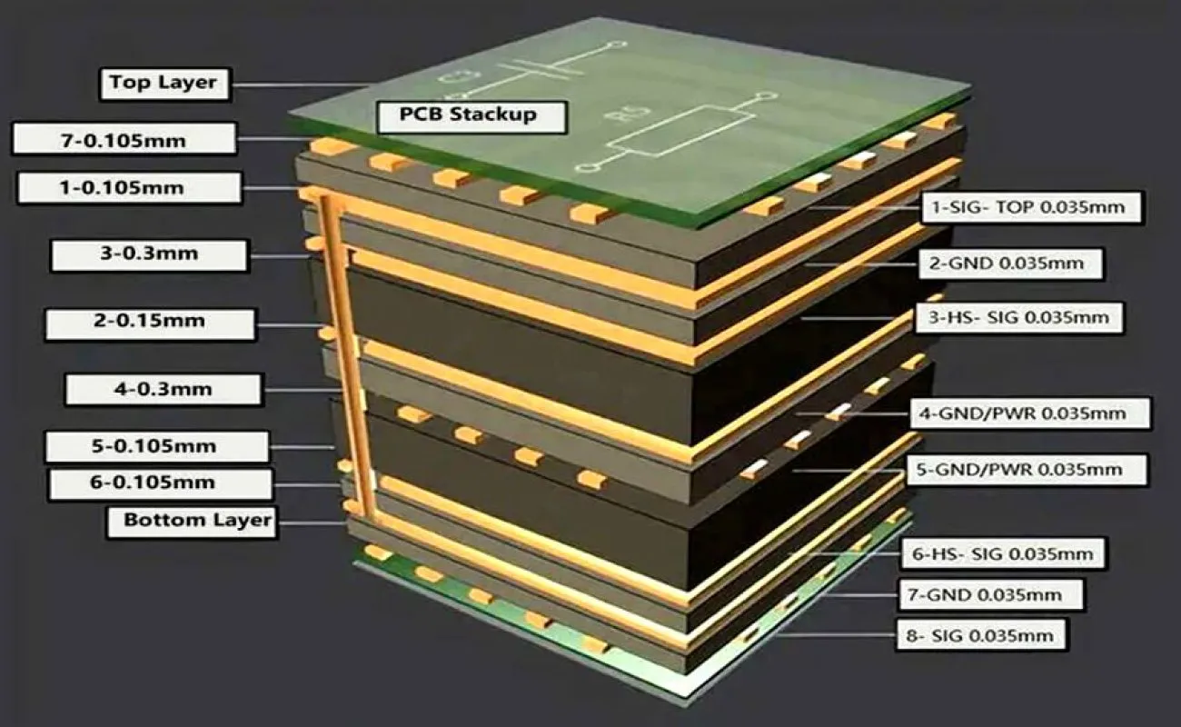
Current carrying capacity depends on trace width, copper thickness, and allowable temperature rise, with heat dissipation occurring through conduction into the board and convection to surrounding air. Voltage withstand capability relies on proper selection of dielectric materials with adequate comparative tracking index and appropriate spacing rules derived from insulation coordination principles. Multilayer stackups allow power and signal layers to be separated, reducing crosstalk while providing dedicated planes for return currents. Thermal vias and copper pours help spread heat from power components such as MOSFETs or diodes to larger areas of the board. Material properties including glass transition temperature and coefficient of thermal expansion must align with expected operating conditions to minimize warpage or cracking during thermal cycling. These mechanisms interact, so changes in one area often affect others.
Practical Solutions and Best Practices
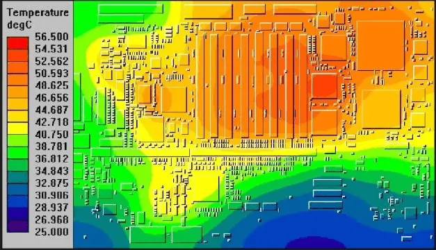
Designers begin by defining voltage and current requirements early, then apply appropriate spacing rules throughout the layout. Increasing copper weight on power layers improves current handling while thermal vias transfer heat to internal planes or heatsinks. Component placement keeps high voltage sections isolated from sensitive control circuitry, often using physical barriers or separate board regions. Conformal coatings or potting compounds provide additional environmental protection when required by the application. Rigorous testing includes hipot verification for insulation integrity and thermal imaging under load to confirm temperature distributions remain within limits. Iterative simulation of electrical, thermal, and mechanical behavior helps identify issues before prototyping.
Safety Standards and Compliance Considerations
Adherence to established standards guides spacing, material qualification, and performance verification for automotive PCBs. IPC-6012E provides qualification and performance specifications for rigid printed boards that support consistent manufacturing outcomes. Proper application of these guidelines helps achieve the necessary insulation coordination and mechanical durability. Standards also inform acceptance criteria during incoming inspection and final testing, reducing variability across production runs.
Conclusion
EV charger PCB design requires simultaneous management of electrical, thermal, and environmental factors to deliver safe and efficient performance. Structured approaches that incorporate appropriate material choices, layout techniques, and verification methods address the primary challenges of high voltage and high current operation. Continued attention to these principles supports reliable charging systems as electric vehicle technology advances.
FAQs
Q1: What are the main considerations in EV charger PCB design for high voltage applications?
A1: High voltage sections require increased creepage and clearance distances along with dielectric materials that resist tracking. Layout practices separate high voltage areas from control circuitry while ensuring adequate insulation coordination. These steps help maintain safety and reliability under automotive operating conditions.
Q2: How does high current PCB design affect thermal management in battery chargers?
A2: High current paths generate heat that must be dissipated through thicker copper, thermal vias, and strategic placement of planes. Without proper thermal design, localized temperature rises can degrade performance or cause failures. Effective heat spreading maintains component temperatures within acceptable ranges during continuous operation.
Q3: Why are automotive PCB requirements stricter for EV chargers than for consumer electronics?
A3: Automotive environments impose vibration, wide temperature swings, and potential moisture exposure that demand enhanced mechanical and environmental robustness. Safety standards for high voltage systems add further requirements for insulation integrity and fault tolerance. These factors drive more rigorous qualification and testing protocols.
Q4: What role do industry standards play in EV charger PCB manufacturing?
A4: Standards such as those from IPC define performance and qualification criteria that promote consistent quality across suppliers. They guide material selection, spacing rules, and acceptance testing to support reliable long term operation. Compliance helps ensure designs meet the safety and durability expectations of automotive applications.





