 ALLPCB


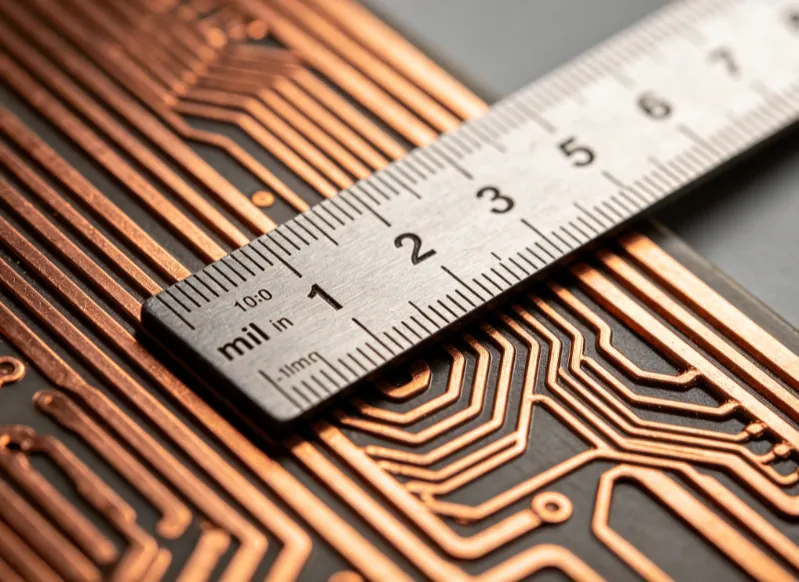
Line width, expressed in mils, forms a foundational element of printed circuit board layouts. Engineers routinely convert design rules and current requirements into this unit because many fabrication facilities in North America still specify tolerances and minimum features in mils. When trace widths deviate from intended values, the resulting PCB design problems can manifest as excessive voltage drop, localized heating, or degraded signal quality. These issues often surface only after prototypes reach testing or field deployment, making early verification essential. Structured review of width calculations against established guidelines helps prevent downstream failures.
Why Trace Width in Mils Matters in PCB Design
Trace width directly governs the current-carrying capacity and thermal behavior of every conductor on a board. Undersized traces increase resistance, which raises power dissipation and can trigger thermal runaway in high-current paths. Oversized traces consume valuable routing space and may force impedance mismatches in controlled-impedance designs. Manufacturing processes introduce tolerances of several mils, so a nominal 10-mil trace can vary enough to affect both power delivery and high-speed signaling. Electric engineers therefore treat width selection as a multi-variable optimization that balances electrical performance, thermal limits, and board real estate.
Technical Principles Behind Trace Width Issues
Current capacity follows relationships outlined in industry standards that correlate conductor cross-section, temperature rise, and allowable current. When designers rely on simplified rules of thumb instead of these relationships, traces may overheat under load or exhibit electromigration over time. Signal integrity suffers when width variations alter characteristic impedance, producing reflections that distort edges and increase bit-error rates. Power delivery networks experience voltage droop when narrow traces create excessive IR drop between regulators and loads. Thermal expansion differences between copper and substrate can also induce mechanical stress at trace corners or vias if widths are not chosen with coefficient-of-thermal-expansion effects in mind.
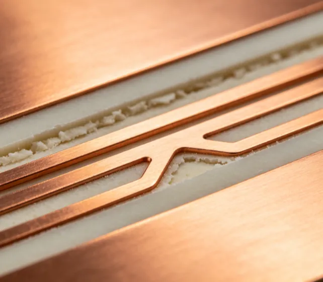
Manufacturing variations compound these electrical concerns. Etch factor, plating thickness, and copper foil weight all influence the final cross-sectional area. A design specifying 8 mils may finish at 6.5–9.5 mils depending on process controls. Such deviations alter both DC resistance and high-frequency skin-effect losses. In multilayer boards, inner-layer traces experience different etch profiles than outer layers, requiring separate width rules. Failure analysis of returned boards frequently reveals that trace-width deviations initiated the sequence of events leading to open circuits or intermittent connections.
Practical Approaches to Resolving Trace Width Problems
Begin every layout by establishing current requirements for each net and applying the relationships defined in IPC-2152 to determine minimum widths at the target temperature rise. Cross-check these values against the spacing rules in IPC-2221 to maintain adequate isolation. Perform a full-board thermal simulation that accounts for copper distribution, airflow, and adjacent heat sources rather than relying on single-trace calculations. When signal integrity is critical, run impedance calculations or field solvers to confirm that the chosen widths produce the required characteristic impedance across the frequency range of interest.
Review fabrication notes with the board house before release to confirm that minimum widths, tolerances, and copper weights align with their process capabilities. Incorporate test coupons on every panel that allow post-fabrication measurement of actual trace widths and resistances. During prototype bring-up, measure voltage drops along power traces under maximum load and compare results to calculated values. If discrepancies appear, inspect cross-sections to quantify actual copper thickness and width. Adjust subsequent revisions by widening critical traces or redistributing current across parallel paths.
Troubleshooting Workflow for Common Failures
When a board exhibits unexpected heating or functional errors, first map the affected nets and compare their widths against the original current calculations. Use infrared imaging to locate hot spots that correlate with narrow traces. Next, perform four-point resistance measurements on suspect traces to quantify deviations from design intent. If resistance is higher than expected, examine the board under magnification for etch undercut or plating voids. For signal-integrity failures, capture eye diagrams or TDR profiles to identify impedance discontinuities that trace back to width variations.
Document each finding with photographs and measurements so that layout rules can be updated for future designs. In many cases, increasing width by two to four mils or adding stitching vias to improve thermal spreading resolves the immediate issue without requiring a complete redesign. When failures recur across multiple builds, revisit the stack-up and copper-weight assumptions that fed the original width calculations.
Key Takeaways for Electric Engineers
Consistent application of width calculations based on recognized standards reduces the incidence of PCB design problems related to trace width issues. Regular verification against measured board characteristics closes the loop between simulation and reality. Power delivery problems and signal integrity troubleshooting both benefit from treating trace width as a controllable variable rather than a fixed input. Systematic failure analysis of width-related defects feeds continuous improvement of design rules and fabrication notes.
FAQs
Q1: How do trace width issues affect signal integrity troubleshooting?
A1: Variations in trace width alter impedance and increase insertion loss, which can cause reflections, ringing, and eye closure in high-speed links. Engineers compare measured impedance profiles against target values derived from the intended width and dielectric properties to isolate the root cause.
Q2: What steps help prevent power delivery problems caused by inadequate trace widths?
A2: Calculate minimum widths using the current-versus-temperature relationships in IPC-2152, then verify voltage drop under worst-case load. Adding parallel traces or increasing copper weight provides margin when space constraints limit single-trace solutions.
Q3: How does PCB failure analysis typically identify line-width defects?
A3: Cross-sectioning and resistance measurements reveal actual conductor dimensions that differ from design files. Thermal imaging and microscopic inspection further correlate physical deviations with observed heating or open-circuit failures.
Q4: Why is it important to specify trace widths in mils during PCB design?
A4: Many North American fabrication processes still quote tolerances and minimum features in mils, so using this unit reduces transcription errors between design rules and shop-floor documentation.
References
IPC-2221 — Generic Standard on Printed Board Design. IPC.
IPC-2152 — Standard for Determining Current Carrying Capacity in Printed Board Design. IPC.
IPC-6012E — Qualification and Performance Specification for Rigid Printed Boards. IPC, 2017.


